
Datasheet


www.ti.com
I
2
CWriteSequence
SCL
SDA
A5
A4
A3 A2
A1
A0
0
ACK
B7 B6 B5 B4 B3 R2 R1 R0
I2C
6
A6
I2C
5
I2C
4
D7 D6 D5 D4 D3 D2 D1 D0
D7
D6 D5 D4 D3 D2 D1 D0
ACK ACK ACK
Programmable I CDevice Address2
SetbyControlRegister2
StartBit=0
SMARTDMDevice
Address
(seeTable1)
00000=Default
11111=BroadcastMode
IndexRegister Address
(Index)
ControlRegisterDataforWrite
(Index)
ControlRegisterDataforWrite
(Index+1)
SCL
SDA
A5 A4 A3 A2
A1
A0 0
ACK
B7 B6 B5 B4 B3 R2 R1 R0
I2C
6
A6 ACK
I2C
5
I2C
4
SCL
SDA
A5
A4 A3
A2
A1
A0 1
ACK
D7 D6 D5 D4 D3 D2 D1 D0
I2C
6
A6
I2C
5
I2C
4
D7 D6 D5 D4 D3 D2 D1 D0
ACK ACK
StartBit=0
Programmable12CDevice Address
SetbyControlRegister2
SMARTDMDevice Address
(seeTable1)
IndexRegister Address
(Index)
StopBit=1
xxxxx=Don'tCare
StartBit=0
Programmable12CDevice Address
SetbyControlRegister2
SMARTDMDevice Address
(seeTable1)
ControlRegisterData
(Index)
ControlRegisterData
(Index+1)
I
2
CReadSequence
TLV320AIC12, TLV320AIC13
TLV320AIC14, TLV320AIC15
TLV320AIC12K, TLV320AIC14K
SLWS115E – OCTOBER 2001 – REVISED JANUARY 2007
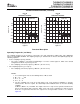
Figure 27. I
2
C Write Sequence
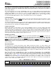
Figure 28. I
2
C Read Sequence
Each AIC has an index register address. To perform a write operation, make the LSB of the first byte as 0 (write)
(see Figure 29 ). During the second byte, the index register address is initialized and mode (broadcast/default) is
set. From the third byte onwards, write data to the control register (given by index register) and increment the
index register until stop or repeated start occurs. For operation, make the LSB of the first byte as 1 (read). From
the second byte onwards, AIC starts transmitting data from the control register (given by the index register) and
increments the index register. For setting the index register perform operation the same as write case for 2
bytes, and then give a stop or repeated start.
• S/Sr -> Start/Repeated Start.
29
Submit Documentation Feedback