
Datasheet


www.ti.com
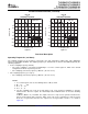
−140
−120
−100
−80
−60
−40
−20
0
20
0 1000 2000 3000 4000 5000 6000 7000 8000
Filter Gain − dB
f − Frequency − Hz
OSR = 256
−140
−120
−100
−80
−60
−40
−20
0
20
0 1000 2000 3000 4000 5000 6000 7000 8000
Filter Gain − dB
f − Frequency − Hz
OSR = 128
Functional Description
Operating Frequencies (see Notes)
TLV320AIC12, TLV320AIC13
TLV320AIC14, TLV320AIC15
TLV320AIC12K, TLV320AIC14K
SLWS115E – OCTOBER 2001 – REVISED JANUARY 2007
TYPICAL CHARACTERISTICS (continued)
DAC FIR DAC FIR
vs vs
FREQUENCY RESPONSE FREQUENCY RESPONSE
Figure 18. Figure 19.
The sampling frequency is the frequency of the frame sync (FS) signal whose falling edge starts digital-data
transfer for both ADC and DAC. The sampling frequency is derived from the master clock (MCLK) input by the
following equations:
• Coarse sampling frequency (default):
– The coarse sampling is selected by programming P = 8 in the control register 4, which is the default
configuration of AIC1x on power-up or reset.
– FS = Sampling (conversion) frequency = MCLK ÷ (16 × M × N × 8)
• Fine sampling frequency (see step 5):
– FS = Sampling (conversion) frequency = MCLK ÷ (16 × M × N × P)
NOTES:
1. Use control register 4 to set the following values of M, N, and P
2. M = 1, 2, . . . , 128
3. N = 1, 2,..., 16
4. P = 1, 2, ..., 8
5. The fine sampling rate needs an on-chip Phase Lock Loop (frequency multiplier) to generate
internal clocks. The PLL requires the relationship between MCLK and P to meet the following
condition:
10 MHz ≤ (MCLK ÷ P) ≤ 25 MHz. The output of the PLL is only used to generate internal clocks
that are needed by the data converters. Other clocks such as the serial interface clocks in master
mode are not generated from the PLL output. The clock generation scheme is as shown in
Figure 20 .
21
Submit Documentation Feedback