Datasheet
Table Of Contents
- TABLE OF CONTENTS
- LIST OF FIGURES
- LIST OF TABLES
- General Description
- Applications
- Features and Benefits
- Application Diagram
- 16-Bit to 20-Bit SAR ADC Family
- Absolute Maximum Ratings
- Package Thermal Characteristics
- Electrical Characteristics
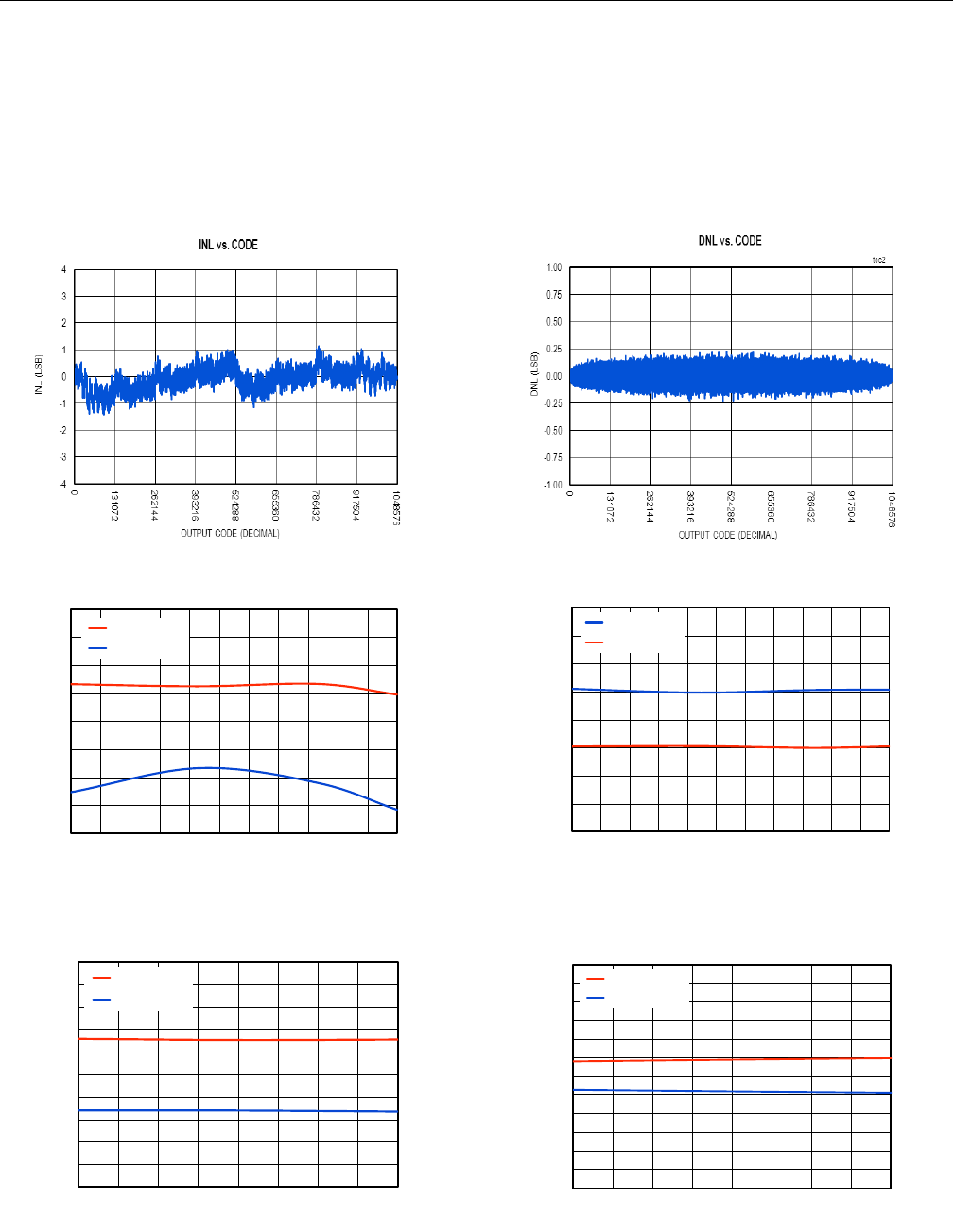
- Typical Operating Characteristics
- Pin Configuration
- Pin Description
- Functional Diagram
- Detailed Description
- Digital Interface
- Register Map
- Typical Application Circuit
- Layout, Grounding, and Bypassing
- Definitions
- Selector Guide
- Ordering Information
- Chip Information
- Package Information
- Revision History
- Figure 1. Signal Ranges
- Figure 2. Simplified Model of Input Sampling Circuit
- Figure 3. Conversion Frame, SAR Conversion, Track and Read Operation
- Figure 4. Ideal Transfer Characteristic
- Figure 5. Read During Track Phase
- Figure 6. Read During SAR Conversion Phase
- Figure 7. Split Read Mode
- Figure 8. SPI Interface Connection
- Figure 9. DIN Timing for Register Write Operations
- Figure 10. Timing Diagram for Data Out Reading After Conversion
- Figure 11. Mode Register Write
- Figure 12. Register Read
- Figure 13. Unipolar Single-Ended Input
- Figure 14. Bipolar Single-Ended Input
- Figure 15. Top Layer Sample Layout
- Table 1. ADC Driver Amplifier Recommendation
- Table 2. Voltage Reference Configurations
- Table 3. MAX11905 External Reference Recommendations
- Table 4. Transfer Characteristic
- Table 5. DOUT Driver Strength

(V
AVDD
= 1.8V, V
DVDD
= 1.8V, V
OVDD
= 1.8V, V
REFVDD
= 3.6V, f
SAMPLE
= 1.6Msps, V
REF
= 3.3V, Internal Ref Buffer On, T
A
= T
MIN
to T
MAX
, unless otherwise noted. Typical values are at T
A
= +25°C.)
-2.0
-1.5
-1.0
-0.5
0.0
0.5
1.0
1.5
2.0
-40 -25 -10 5 20 35 50 65 80 95 110 125
DNL (LSB)
TEMPERATURE (
o
C)
DNL vs. TEMPERATURE
MAX DNL (LSB)
MIN DNL (LSB)
toc4
-3
-2
-1
0
1
2
3
1.70 1.73 1.75 1.78 1.80 1.83 1.85 1.88 1.90
DNL (LSB)
V
AVDD
(V)
DNL vs. AVDD SUPPLY VOLTAGE
MAX DNL (LSB)
MIN DNL (LSB)
toc6
-4
-3
-2
-1
0
1
2
3
4
-40 -25 -10 5 20 35 50 65 80 95 110 125
INL (LSB)
TEMPERATURE (
o
C)
INL vs. TEMPERATURE
MAX INL (LSB)
MIN INL (LSB)
toc3
-5
-4
-3
-2
-1
0
1
2
3
4
5
1.70 1.73 1.75 1.78 1.80 1.83 1.85 1.88 1.90
INL (LSB)
V
AVDD
(V)
INL vs. AVDD SUPPLY VOLTAGE
MAX INL (LSB)
MIN INL (LSB)
toc5
toc1
MAX11905 20-Bit, 1.6Msps, Low-Power, Fully Differential
SAR ADC
Maxim Integrated
│
8
www.maximintegrated.com
Typical Operating Characteristics


