
Datasheet


TPS7A4700
TPS7A4701
www.ti.com
SBVS204E –JUNE 2012–REVISED JANUARY 2014
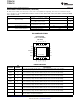
THERMAL INFORMATION
TPS7A47xx
THERMAL METRIC
(1)
RGW UNITS
20 PINS
θ
JA
Junction-to-ambient thermal resistance 32.5
θ
JCtop
Junction-to-case (top) thermal resistance 27
θ
JB
Junction-to-board thermal resistance 11.9
°C/W
ψ
JT
Junction-to-top characterization parameter 0.3
ψ
JB
Junction-to-board characterization parameter 11.9
θ
JCbot
Junction-to-case (bottom) thermal resistance 1.7
(1) For more information about traditional and new thermal metrics, see the IC Package Thermal Metrics application report, SPRA953.
ELECTRICAL CHARACTERISTICS
At –40°C ≤ T
J
≤ +125°C; V
IN
= V
OUT(NOM)
+ 1.0 V or V
IN
= 3.0 V (whichever is greater); V
EN
= V
IN
; I
OUT
= 0 mA; C
IN
=10 µF;
C
OUT
= 10 µF; C
NR
= 10 nF; SENSE/FB tied to OUT; and 0P1V, 0P2V, 0P4V, 0P8V, 1P6V, 3P2V, 6P4V1, 6P4V2 pins OPEN,
unless otherwise noted.
PARAMETER TEST CONDITIONS MIN TYP MAX UNIT
V
IN
Input voltage range 3 35 V
V
IN
rising 2.67 V
V
UVLO
Under-voltage lockout threshold
V
IN
falling 2.5 V
V
UVLO_HYS
Under-voltage lockout hysteresis 177 mV
TPS7A4700, TPS7A4701 using ANYOUT
V
OUT
V
option
V
NR
Noise reduction pin voltage
TPS7A4701 in adjustable mode only 1.4 V
TPS7A4700,
TPS7A4701
using 1.4 20.5 V
ANYOUT
V
IN
≥ V
OUT(NOM)
+ 1.0 V or 3V
option
Output voltage range (whichever is greater),
C
OUT
= 20 µF
TPS7A4701
V
OUT
using
1.4 34 V
adjustable
option
Nominal accuracy T
J
= +25°C, C
OUT
= 20 µF –1.0 1.0 %V
OUT
V
OUT(NOM)
+ 1.0 V ≤ V
IN
≤ 35 V,
Overall accuracy –2.5 2.5 %V
OUT
0 mA ≤ I
OUT
≤ 1 A, C
OUT
= 20 µF
V
REF
Reference voltage V
REF
= V
FB
, TPS7A4701 only 1.4 V
ΔV
O(ΔVI)
Line regulation V
OUT(NOM)
+ 1.0 V ≤ V
IN
≤ 35 V 0.092 %V
OUT
ΔV
O(ΔIO)
Load regulation 0 mA ≤ I
OUT
≤ 1 A 0.3 %V
OUT
V
IN
= 95% V
OUT(NOM)
, I
OUT
= 0.5 A 216 mV
V
DO
Dropout voltage
V
IN
= 95% V
OUT(NOM)
, I
OUT
= 1 A 307 450 mV
I
CL
Current limit V
OUT
= 90% V
OUT(NOM)
1 1.26 A
I
OUT
= 0 mA 0.58 1.0 mA
I
GND
Ground pin current
I
OUT
= 1 A 6.1 mA
V
EN
= 0.4 V 2.55 8 µA
I
SHDN
Shutdown supply current
V
EN
= 0.4 V, V
IN
= 35 V 3.04 60 µA
V
EN
= V
IN
0.78 2 µA
I
EN
Enable pin current
V
IN
= V
EN
= 35 V 0.81 2 µA
I
FB
Feedback pin current 350 nA
V
+EN(HI)
Enable high-level voltage 2.0 V
IN
V
V
+EN(LO)
Enable low-level voltage 0.0 0.4 V
Copyright © 2012–2014, Texas Instruments Incorporated Submit Documentation Feedback 3
Product Folder Links: TPS7A4700 TPS7A4701