
Datasheet


SLVS519A − MAY 2004 − REVISED OCTOBER 2004
www.ti.com
8
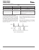
FUNCTIONAL BLOCK DIAGRAM
VBIAS
PH
BOOT
VIN
LSG
VBIAS
Error
Amplifier
2x Oscillator
PWM Ramp
(FeedFoward)
SYNC
RT
VSENSE
PWM
Comparator
Reference
System
ENA
VBIAS2
Hiccup
Timer
Thermal
Shutdown
Current Limit
Hiccup
Hiccup
UVLO
UVLO
UVLO
1.2V
Bias + Drive
Regulator
PWRGD
AGNDPGND
Rising
Edge
Delay
VBIAS
COMP
Adaptive Deadtime
and
Control Logic
97% Ref
POWERPAD
VSENSE
UVLO
S
R
Q
320 kΩ
125 kΩ
(1)
5 µA
(1)
75 kΩ for the TPS54357
Z3
Z1
Z2
Z5
Z4
TPS5435X
DETAILED DESCRIPTION
Undervoltage Lockout (UVLO)
The undervoltage lockout (UVLO) system has an internal
voltage divider from VIN to AGND. The defaults for the
start/stop values are labeled VIN and given in Table 1. The
internal UVLO threshold can be overridden by placing an
external resistor divider from VIN to ground. The internal
divider values are approximately 320 kΩ for the high side
resistor and 125 kΩ for the low side resistor. The divider
ratio (and therefore the default start/stop values) is quite
accurate, but the absolute values of the internal resistors
may vary as much as 15%. If high accuracy is required for
an externally adjusted UVLO threshold, select lower value
external resistors to set the UVLO threshold. Using a 1-kΩ
resistor for the low side resistor (R2 see Figure 1) is
recommended. Under no circumstances should the UVLO
pin be connected directly to VIN.
Table 1. Start/Stop Voltage Threshold
START VOLTAGE THRESHOLD STOP VOLTAGE THRESHOLD
VIN (Default)
TPS54352−6 4.49 3.69
VIN (Default)
TPS54357 6.65 5.45
UVLO 1.24 1.02
The equations for selecting the UVLO resistors are:
R1
VIN(start) 1kW
1.24 V
1kW
VIN(stop)
(R1 1kW) 1.02 V
1kW
(1)
(2)