
Datasheet


SLVS519A − MAY 2004 − REVISED OCTOBER 2004
www.ti.com
7
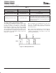
PIN ASSIGNMENTS
1
2
3
4
5
6
7
8
16
15
14
13
12
11
10
9
VIN
VIN
UVLO
PWRGD
RT
SYNC
ENA
COMP
BOOT
PH
PH
LSG
VBIAS
PGND
AGND
VSENSE
PWP PACKAGE
(TOP VIEW)
THERMAL
PAD
NOTE:
If there is not a Pin 1 indicator, turn device to enable
reading the symbol from left to right. Pin 1 is at the lower
left corner of the device.
Terminal Functions
TERMINAL
DESCRIPTION
NO. NAME
DESCRIPTION
1, 2 VIN Input supply voltage, 4.5 V to 20 V. Must bypass with a low ESR 10-µF ceramic capacitor. Place cap as close to device as
possible; see Figure 23 for an example.
3 UVLO Undervoltage lockout pin. Connecting an external resistive voltage divider from VIN to the pin will override the internal
default VIN start and stop thresholds.
4 PWRGD Power good output. Open drain output. A low on the pin indicates that the output is less than the desired output voltage.
There is an internal rising edge filter on the output of the PWRGD comparator.
5 RT Frequency setting pin. Connect a resistor from RT to AGND to set the switching frequency. Connecting the RT pin to
ground or floating will set the frequency to an internally preselected frequency.
6 SYNC Bidirectional synchronization I/O pin. SYNC pin is an output when the RT pin is floating or connected low. The output is a
falling edge signal out of phase with the rising edge of PH. SYNC may be used as an input to synchronize to a system clock
by connecting to a falling edge signal when an RT resistor is used. See 180° Out of Phase Synchronization operation in the
Application Information section. In ALL cases, a 10 kΩ resistor Must be tied to the SYNC pin in parallel with ground. For
information on how to extend slow start, see the Enable (ENA) and Internal Slow Start section on page 9.
7 ENA Enable. Below 0.5 V, the device stops switching. Float pin to enable.
8 COMP Error amplifier output. Do NOT connect ANYTHING to this pin.
9 VSENSE Feedback pin
10 AGND Analog ground—internally connected to the sensitive analog ground circuitry. Connect to PGND and PowerPAD.
11 PGND Power ground—Noisy internal ground—Return currents from the LSG driver output return through the PGND pin. Connect
to AGND and PowerPAD.
12 VBIAS Internal 8.0-V bias voltage. A 1.0-µF ceramic bypass capacitance is required on the VBIAS pin.
13 LSG Gate drive for optional low side MOSFET. Connect gate of n-channel MOSFET for a higher efficiency synchronous buck
converter configuration. Otherwise, leave open and connect schottky diode from ground to PH pins.
14, 15 PH Phase node—Connect to external L−C filter.
16 BOOT Bootstrap capacitor for high side gate driver. Connect a 0.1-µF ceramic capacitor from BOOT to PH pins.
PowerPAD PGND and AGND pins must be connected to the exposed pad for proper operation. See Figure 23 for an example PCB
layout.