
Datasheet


TLV571
2.7 V TO 5.5 V, 1-CHANNEL, 8-BIT,
PARALLEL ANALOG-TO-DIGITAL CONVERTER
SLAS239A – SEPTEMBER 1999 – REVISED FEBRUARY 2000
6
POST OFFICE BOX 655303 • DALLAS, TEXAS 75265
detailed description (continued)
reference voltage input
The TLV571 has two reference input pins: REFP and REFM. The voltage levels applied to these pins establish
the upper and lower limits of the analog inputs to produce a full-scale and zero-scale reading respectively. The
values of REFP, REFM, and the analog input should not exceed the positive supply or be less than GND
consistent with the specified absolute maximum ratings. The digital output is at full scale when the input signal
is equal to or higher than REFP and is at zero when the input signal is equal to or lower than REFM.
sampling/conversion
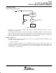
All sampling, conversion, and data output in the device are started by a trigger. This could be the RD, WR, or
CSTART signal depending on the mode of conversion and configuration. The rising edge of RD, WR, and
CSTART signal are extremely important, since they are used to start the conversion. These edges need to stay
close to the rising edge of the external clock (if it is used as CLK). The minimum setup and hold time with respect
to the rising edge of the external clock should be 5 ns minimum. When the internal clock is used, this is not an
issue since these two edges will start the internal clock automatically. Therefore, the setup time is always met.
Software controlled sampling lasts 6 clock cycles. This is done via the CLK input or the internal oscillator if
enabled. The input clock frequency can be 1 MHz to 20 MHz, translating into a sampling time from 0.6 µs to
0.3 µs. The internal oscillator frequency is 9 MHz minimum (ocillator frequency is between 9 MHz to 22 MHz),
translating into a sampling time from 0.6 µs to 0.3 µs. Conversion begins immediately after sampling and lasts
10 clock cycles. This is again done using the external clock input (1 MHz–20 MHz) or the internal oscillator
(9 MHz minimum) if enabled. Hardware controlled sampling, via CSTART
, begins on falling CSTART lasts the
length of the active CSTART
signal. This allows more control over the sampling time, which is useful when
sampling sources with large output impedances. On rising CSTART, conversion begins. Conversion in
hardware controlled mode also lasts 10 clock cycles. This is done using the external clock input (1 MHz–20 MHz)
or the internal oscillator (9 MHz minimum) as is the case in software controlled mode.
NOTE: t
su
= setup time, t
h
= hold time
ExtClk
WR
RD
CSTART
t
su(WRH_EXTCLKH)
≥5 ns
t
h(WRL_EXTCLKH)
≥5 ns
t
h(RDL_EXTCLKH)
≥5 ns
t
d(EXTCLK_CSTARTL)
≥5 ns
t
h(CSTARTL_EXTCLKH)
≥5 ns
t
su(CSTARTH_EXTCLKH)
≥5 ns
OR
OR
t
su(RDH_EXTCLKH)
≥5 ns
Figure 3. Trigger Timing – Software Start Mode Using External Clock