
Datasheet


TLV571
2.7 V to 5.5 V, 1-CHANNEL, 8-BIT
RARALLEL ANALOG-TO-DIGITAL CONVERTER
SLAS239A – SEPTEMBER 1999 – REVISED FEBRUARY 2000
10
POST OFFICE BOX 655303 DALLAS, TEXAS 75265
•
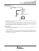
software START conversion
external clock
With CS low and WR low, data is written into the ADC. Sampling begins at the rising edge of WR. The conversion process begins 6 clocks
after sampling begins. At the end of conversion, the INT goes low telling the host that conversion is ready to be read out. EOC B low during
the conversion. The external clock is active and used as the reference at all times. With this mode, WR and RD should not be applied at the
rising edge of the clock (see Figure 3).
Auto Powerdown
CLK
CS
WR
RD
D[0:7]
INT
EOC
Config
Data
ADC Data ADC Data
t
su(CSL_WRL)
t
h(WRH_CSH)
t
su(DAV_WRH)
t
h(WRH_DAV)
t
c
t
su(CSL_RDL)
t
h(RDH_CSH)
t
en(RDL_DAV)
t
dis(RDH_DAV)
t
c
t
t
en(RDL_DAV)
015671516
OR
su(CSL_RDL)
t
(sample)
t
(sample)
04515
Figure 6. Input Conversion – Software Start, External Clock