
Datasheet


LM7341
www.ti.com
SNOSAW9B –MAY 2008–REVISED MARCH 2013
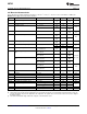
2.7V Electrical Characteristics
Unless otherwise specified, all limits ensured for T
A
= 25°C, V
+
= 2.7V, V
−
= 0V, V
CM
= 0.5V, V
OUT
= 1.35V and R
L
> 1 MΩ to
1.35V. Boldface limits apply at the temperature extremes
Symbol Parameter Conditions Min
(1)
Typ
(2)
Max
(1)
Units
V
OS
Input Offset Voltage V
CM
= 0.5V and V
CM
= 2.2V −4 ±0.2 +4
mV
−5 +5
TCV
OS
Input Offset Voltage Temperature Drift ±2 μV/°C
I
B
Input Bias Current V
CM
= 0.5V −180 −90
−200
nA
V
CM
= 2.2V 30 60
70
I
OS
Input Offset Current V
CM
= 0.5V and V
CM
= 2.2V 1 40
nA
50
CMRR Common Mode Rejection Ratio 0V ≤ V
CM
≤ 1.0V 82 106
80
dB
0V ≤ V
CM
≤ 2.7V 62 80
60
PSRR Power Supply Rejection Ratio 2.7V ≤ V
S
≤ 30V 86 106 dB
V
CM
= 0.5V 84
CMVR Common Mode Voltage Range CMRR > 60 dB −0.3 0.0
V
2.7 3.0
A
VOL
Open Loop Voltage Gain 0.5V ≤ V
O
≤ 2.2V 12 65
V/mV
R
L
= 10 kΩ to 1.35V 8
V
OUT
Output Voltage Swing R
L
= 10 kΩ to 1.35V 50 120
High V
ID
= 100 mV 150
R
L
= 2 kΩ to 1.35V 95 150
V
ID
= 100 mV 200
mV from
either rail
Output Voltage Swing R
L
= 10 kΩ to 1.35V 55 120
Low V
ID
= −100 mV 150
R
L
= 2 kΩ to 1.35V 100 150
V
ID
= −100 mV 200
I
OUT
Output Current Sourcing, V
OUT
= 0V 6 12
V
ID
= 200 mV 4
mA
Sinking, V
OUT
= 0V 5 10
V
ID
= −200 mV 3
I
S
Supply Current V
CM
= 0.5V and V
CM
= 2.2V 0.6 0.9
mA
1.0
SR Slew Rate ±1V Step 1.5 V/μs
GBW Gain Bandwidth f = 100 kHz, R
L
= 100 kΩ 3.6 MHz
e
n
Input Referred Voltage Noise Density f = 1 kHz 35 nV/√Hz
i
n
Input Referred Voltage Noise Density f = 1 kHz 0.28 pA/√Hz
THD+N Total Harmonic Distortion + Noise f = 10 kHz −66 dB
t
PD
Propagation Delay Overdrive = 50 mV
(3)
4
µs
Overdrive = 1V
(3)
3
t
r
Rise Time 20% to 80%
(3)
1 µs
t
f
Fall Time 80% to 20%
(3)
1 µs
(1) All limits are specified by testing or statistical analysis.
(2) Typical values represent the most likely parametric norm as determined at the time of characterization. Actual typical values may vary
over time and will also depend on the application and configuration. The typical values are not tested and are not ensured on shipped
production material.
(3) The maximum differential voltage between the input pins is V
IN
Differential = ±15V.
Copyright © 2008–2013, Texas Instruments Incorporated Submit Documentation Feedback 3
Product Folder Links: LM7341