
Datasheet
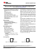


POWER-ON
RESET
DAC
REGISTER
INPUT
CONTROL
LOGIC
10-BIT DAC
10
10
POWER-DOWN
CONTROL
LOGIC
BUFFER
1k 100k
SCLK
D
IN
SYNC
REF(+) REF(-)
V
A
GND
DAC101S101
V
OUT
DAC101S101, DAC101S101-Q1
SNAS321F –JUNE 2005–REVISED MARCH 2013
www.ti.com
Block Diagram
PIN DESCRIPTIONS
SOT
VSSOP
(SOT-23) Symbol Description
Pin No.
Pin No.
1 4 V
OUT
DAC Analog Output Voltage.
2 8 GND Ground reference for all on-chip circuitry.
3 1 V
A
Power supply and Reference input. Should be decoupled to GND.
Serial Data Input. Data is clocked into the 16-bit shift register on the falling
4 7 D
IN
edges of SCLK after the fall of SYNC.
Serial Clock Input. Data is clocked into the input shift register on the falling
5 6 SCLK
edges of this pin.
Frame synchronization input for the data input. When this pin goes low, it
enables the input shift register and data is transferred on the falling edges
6 5 SYNC of SCLK. The DAC is updated on the 16th clock cycle unless SYNC is
brought high before the 16th clock, in which case the rising edge of SYNC
acts as an interrupt and the write sequence is ignored by the DAC.
2, 3 NC No Connect. There is no internal connection to these pins.
These devices have limited built-in ESD protection. The leads should be shorted together or the device placed in conductive foam
during storage or handling to prevent electrostatic damage to the MOS gates.
2 Submit Documentation Feedback Copyright © 2005–2013, Texas Instruments Incorporated
Product Folder Links: DAC101S101 DAC101S101-Q1