
Instruction Manual


_________________________________________________________________________________________________________ 14-14
MAXQ7667 User’s Guide
14.5.5 Analog Input Protection
Internal ESD protection diodes limit all analog inputs to AVDD and AGND, allowing the inputs to swing from (AGND - 0.3V) to (AVDD
+ 0.3V) without damage. However, for accurate conversions near full scale, the inputs should not exceed AVDD by more than +50mV
or be lower than AGND by -50mV. Input voltages beyond AGND - 0.3V and AVDD + 0.3V forward bias the internal protection diodes.
In this situation, limit the forward diode current to 50mA to avoid damaging the MAXQ7667.
The common-mode analog input range or absolute analog input range for the MAXQ7667 is specified from AGND to AVDD. Signals
may run outside of that range but will be interpreted as an overrange (ADC data output set to 0xFFF in unipolar mode and to 0x7FF in
bipolar mode) or an underrange condition (ADC data output set to 0x000 in unipolar mode and to 0x800 in bipolar mode). Analog input
signals cannot go outside of the ABS max input signal ratings of +0.3V above AVDD or -0.3V below AGND.
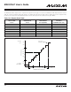
Figure 14-6 shows the common-mode or absolute analog input range as specified with a selected REFADC value. In unipolar input
configuration (SARBIP = 0 in the SARC register) the output data coding of the ADC is straight binary. It is recommended that the unipo-
lar mode be used with a single-ended input configuration (SARDIF = 0 in the SARC register) where analog input signals are referenced
to the AGND pin.
In bipolar input configuration (SARBIP = 1, register bit location SARC.7) the output data coding of the ADC is two’s complement. Bipolar
mode is commonly used with a differential analog input configuration (SARDIF = 1, register bit location SARC.8) where the analog input
signals are referenced to their complementary analog input (AIN+/-) pin. Figure 14-7 shows how a negative ADC value is created. The
absolute voltage of each analog input signal must be within the MAXQ7667 supply range so as to satisfy the critical absolute maximum
tolerance ratings of the analog inputs, and must also be within the REF range to produce useful information from the ADC.
Figure 14-7. Analog Input Range Measuring a Negative Analog Input Value
REF
REF MAX INPUT = AVDD
AGND
AGND - 0.3V
AVDD
AVDD + 0.3V
ABS MAX+
ABS MAX-
AIN-
AIN+
ADCIN = (AIN+ - AIN-)
REF MIN INPUT = AGND
DIFFERENTIAL
ANALOG
INPUT
ANALOG INPUT
VOLTAGE RANGE
14.5.6 ADC Clock
The MAXQ7667 ADC clock frequency is controlled by the SARCD[1:0] bits in the OSCC control register and the system clock speed.
These bits determine the ADC clock frequency (ADCCLK) that is divided down from the system clock. See
Section 15 for further details
on the system clock. The MAXQ7667 ADC uses the divided system clock to clock the multiplexer front-end selection, track and hold
acquisition, and each step of the successive approximation conversion.
Figure 14-6. Analog Input Range Measuring a Positive Analog Input Value
REF
REF MAX INPUT = AVDD
AGND
AGND - 0.3V
AVDD
AVDD + 0.3V
ABS MAX+
ABS MAX-
AIN+
AIN-
ADCIN = (AIN+ - AIN-)
REF MIN INPUT = AGND
DIFFERENTIAL
ANALOG
INPUT
ANALOG INPUT
VOLTAGE RANGE