
Datasheet


MAX548A/MAX549A/MAX550A
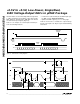
function. Data is clocked in starting with unassigned bit
1 (UB1), followed by the remaining control bits and the
DAC data byte. The data byte’s LSB (D0) is the last bit
clocked into the input register (Figure 2).
Table 5 is an example of a 16-bit input word that per-
forms the following functions:
• Loads 80 hex (128 decimal) into the DAC input regis-
ter (DAC A for the MAX548A/MAX549A)
• Updates the DAC register(s) on CS’s rising edge.
Table 6 shows how to calculate the output voltage
based on the input code. Figure 3 gives detailed timing
information.
+2.5V to +5.5V, Low-Power, Single/Dual,
8-Bit Voltage-Output DACs in µMAX Package
8 _______________________________________________________________________________________
DIN
SCLK
1 8 9 16
LDAC
MAX548A/
MAX550A
ONLY
UB1 UB2
UB3
C2 C1
C0
A1 A0 D7
D6
D5 D4 D3 D2
D1
D0
OPTIONAL
PAUSE
CS
INSTRUCTION
EXECUTED
Figure 2. Serial-Interface Timing Diagram
CS
SCLK
DIN
t
DS
t
DH
t
CL
t
CH
t
CSS0
t
CSH0
t
LDAC
t
CSW
t
CSH1
t
CSS1
t
CSLD
LDAC
Figure 3. Detailed Serial-Interface Timing Diagram