
Datasheet


edge on CS programs the DAC. The input registers can
be loaded independently or simultaneously without
updating the DAC registers. This allows both DAC reg-
isters to be updated simultaneously with different digital
values. The DAC outputs reflect the data stored in the
DAC registers. LDAC can be used to asynchronously
update the DAC registers independently of CS
(MAX548A/MAX550A). With C1 set high, setting C0 in
the control word forces the DAC register(s) to be
updated on LDAC’s falling edge, rather than CS’s rising
edge (Table 1).
Initialization
The MAX548A/MAX549A/MAX550A have an internal
power-on reset. At power-up, all internal registers are
reset to zero; therefore, an initialization write sequence
is not necessary.
Serial-Input Data Format and Control Codes
The control byte determines which input registers/DAC
registers are updated (Table 1). The DAC input regis-
ters are updated on the rising edge of CS. The DAC
registers can be updated on CS’s rising edge or on
LDAC’s falling edge after CS goes high. Bit C0 of the
control byte determines how the DAC registers are
updated for the MAX548A/MAX550A. The MAX549A
has no LDAC pin; the DAC registers are always up-
dated on CS’s rising edge (C0 in the control byte has
no effect).
Tables 2, 3, and 4 list the serial-input command format
for the MAX548A, MAX549A, and MAX550A, respec-
tively. The 16-bit input word consists of an 8-bit control
byte and an 8-bit data byte. The control byte is not
decoded internally. Every control bit performs one
MAX548A/MAX549A/MAX550A
+2.5V to +5.5V, Low-Power, Single/Dual,
8-Bit Voltage-Output DACs in µMAX Package
_______________________________________________________________________________________ 7
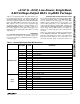
UB3 X Unassigned Bit 3
C2 1 Power-Down Mode
C2 0 Power-Up Mode
C1 1 DAC Register Load Operation Enabled
C0 1
DAC Register Updated on LDAC’s Falling Edge (MAX549A = Don’t Care)
C0 0
DAC Register Updated on CS’s Rising Edge
C1 0 DAC Register Load Operation Disabled
A1 1 Address DAC B (MAX550A = Don’t Care)
A0 1 Address DAC A
A0
UB2
0 Do Not Address DAC A
D6 — DAC Data Bit 6
D4
X
— DAC Data Bit 4
D5
Unassigned Bit 2
STATE
— DAC Data Bit 5
D7 — DAC Data Bit 7 (MSB)
A1 0 Do Not Address DAC B (MAX550A = Don’t Care)
D2
OPERATION
— DAC Data Bit 2
D0**
DATA
BYTE
— DAC Data Bit 0 (LSB)
D1 — DAC Data Bit 1
D3 — DAC Data Bit 3
Table 1. Control-Byte/Input-Word Bit Definitions
X = Don’t care *
Clocked in first
**
Clocked in last
UB1* X Unassigned Bit 1
CONTROL BYTE
BIT NAME