
Datasheet


MAX5060/MAX5061
0.6V to 5.5V Output, Parallelable,
Average-Current-Mode DC-DC Controllers
10 ______________________________________________________________________________________
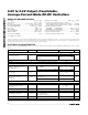
Pin Description
PIN
MAX5060 MAX5061
NAME FUNCTION
13PGND
Power Ground. Connect PGND, low-side synchronous MOSFET’s source, and
V
DD
(MAX5060)/V
CC
(MAX5061) bypass capacitor returns together.
2, 7 8 N.C. No Connection. Not internally connected.
34 DL Low-Side Gate-Driver Output. Synchronous MOSFET gate driver.
45BST
Boost Flying-Capacitor Connection. Reservoir capacitor connection for the high-
side MOSFET driver supply. Connect a 0.47µF ceramic capacitor between BST
and LX.
56 LX
Inductor Connection. Source connection for the high-side MOSFETs. Also serves
as the return terminal for the high-side driver.
67 DH High-Side Gate-Driver Output. Drives the gate of the high-side MOSFET.
8, 22, 25 16 SGND
Signal Ground. Ground connection for the internal control circuitry. Connect
SGND and PGND together at one point near the input bypass capacitor return.
9—CLKOUT
Oscillator Output. Rising edge of CLKOUT is phase-shifted from rising edge of
DH by 180°.
10 — PGOOD
Power-Good Output. PGOOD is an open-drain output that goes low when the
programmed output voltage falls out of regulation. The power-good comparator
threshold is 90% of the programmed output voltage.
11 — EN
Output Enable. Drive EN high or leave unconnected for normal operation. Drive
EN low to shut down the power drivers. EN has an internal 15µA pullup current.
Connect a capacitor from EN to SGND to program the hiccup mode duty cycle.
12 — RT/SYNC
Switching Frequency Programming and Chip-Enable Input. Connect a resistor
from RT/SYNC to SGND to set the internal oscillator frequency. Drive RT/SYNC
externally to synchronize the switching frequency with system clock.
13 — V_IOUT
Voltage-Source Output Proportional to the Output Load Current. The voltage at
V_IOUT is 135 x I
LOAD
x R
S
.
14 10 LIM
Current-Limit Setting Input. Connect a resistor from LIM to SGND to set the
hiccup current-limit threshold. Connect a capacitor from LIM to SGND to ignore
short output overcurrent pulses.
15 — OVI
Overvoltage Protection Circuit Input. Connect OVI to DIFF. When OVI exceeds
+12.7% above the programmed output voltage, DH is latched low and DL is
latched high. Toggle EN low to high or recycle the power to reset the latch.
16 11 CLP
Current-Error-Amplifier Output. Compensate the current loop by connecting an
RC network to ground.