
Datasheet


SLUS274A – JANUARY 1999 – REVISED APRIL 2003
11
www.ti.com
APPLICATION INFORMATION
Once t
START
is calculated, the power limit feature of the UCCx913 must be addressed and component values
derived. Assuming the designer chooses to limit the maximum allowable average power that is associated with
the circuit breaker, the power limiting resistor, R
PL
, can be easily determined by the following:
R
PL
+
P
FET(avg)
1 mA I
MAX
where a minimum R
PL
exists defined by
R
PL(min)
+
|VSS|
10mA
Finally, after computing the aforementioned variables, the minimum timing capacitor can be derived for a current
source load with the following equation.
C
T(min)
+
t
START
ǒ
98 mA R
PL
) |VSS| * 10 V
Ǔ
4V R
PL
The minimum timing capacitor can be derived for a resistive load with the following equation.
C
T(min)
+
t
START
ǒ
49 mA R
PL
) |VSS| * 5V* I
MAX
R
OUT
Ǔ
) R
OUT
C
OUT
|VSS|
2V R
PL
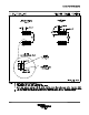
Figure 4. Possible Level Shift Circuitry Interface
UDG–99003
SHUTDOWN
SD/FLT7
R4
R3
VSS
LEVEL SHIFT
LOCAL VDD
LOCAL GND
FAULT OUT
UCC2913
UCC3913
0
2.5
0
75
5.0
10.0
7.5
12.5
17.5
15.0
20.0
25.0
22.5
25 50 100 175125 150 200
Figure 5
I
MAX
= 4 A
R
PL
= ∞
V
FET
– MOSFET Voltage– V
P
AVG
– Average Power Dissipation– W
AVERAGE POWER DISSIPATION
vs
MOSFET VOLTAGE
R
PL
= 10 MΩ
R
PL
= 5 MΩ
R
PL
= 2 MΩ
R
PL
= 1 MΩ
R
PL
= 500 kΩ
R
PL
= 200 kΩ
(16)
(17)
(18)
(19)