
Datasheet


TLV2332, TLV2332Y, TLV2334, TLV2334Y
LinCMOS LOW-VOLTAGE MEDIUM-POWER
OPERATIONAL AMPLIFIERS
SLOS189 – FEBRUARY 1997
8
POST OFFICE BOX 655303 • DALLAS, TEXAS 75265
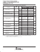
TLV2334I electrical characteristics at specified free-air temperature
†
TLV2334I
PARAMETER TEST CONDITIONS
T
A
†
V
DD
= 3 V V
DD
= 5 V
UNIT
A
MIN TYP MAX MIN TYP MAX
V
IO
In
p
ut offset voltage
V
O
= 1 V, V
IC
= 1 V,
R
S
50 Ω
25°C 0.6 10 1.1 10
mV
V
IO
Inp
u
t
offset
v
oltage
R
S
=
50
Ω
,
R
L
= 100 kΩ
Full range 12 12
mV
α
VIO
Average temperature coefficient
of input offset voltage
25°C to
85°C
1 1.7 µV/°C
I
IO
In
p
ut offset current (see Note 4)
V
O
=1V V
IC
=1V
25°C 0.1 0.1
p
A
I
IO
Inp
u
t
offset
c
u
rrent
(see
Note
4)
V
O
=
1
V
,
V
IC
=
1
V
85°C 22 1000 24 1000
pA
I
IB
In
p
ut bias current (see Note 4)
V
O
=1V V
IC
=1V
25°C 0.6 0.6
p
A
I
IB
Inp
u
t
bias
c
u
rrent
(see
Note
4)
V
O
=
1
V
,
V
IC
=
1
V
85°C 175 2000 200 2000
pA
25
°
C
–0.2
to
–0.3
to
–0.2
to
–0.3
to
V
V
ICR
Common-mode input voltage
25°C
t
o
2
t
o
2.3
t
o
4
t
o
4.2
V
V
ICR
g
range (see Note 5)
Full range
–0.2
to
1.8
–0.2
to
3.8
V
V
OH
High level out
p
ut voltage
V
IC
= 1 V,
V
ID
100 mV
25°C 1.75 1.9 3.2 3.9
V
V
OH
High
-
le
v
el
o
u
tp
u
t
v
oltage
V
ID
=
100
m
V
,
I
OH
= –1 mA
Full range 1.7 3
V
V
OL
Low level out
p
ut voltage
V
IC
= 1 V,
V
ID
100 mV
25°C 115 150 95 150
mV
V
OL
Lo
w-
le
v
el
o
u
tp
u
t
v
oltage
V
ID
= –
100
m
V
,
I
OL
= 1 mA
Full range 190 190
mV
A
VD
Large-signal differential
V
IC
= 1 V,
R
L
100 kΩ
25°C 25 83 25 170
V/mV
A
VD
gg
voltage amplification
R
L
=
100
kΩ
,
See Note 6
Full range 15 15
V/mV
CMRR
Common mode rejection ratio
V
O
= 1 V,
V
IC
V
ICR
min
25°C 65 92 65 91
dB
CMRR
Common
-
mode
rejection
ratio
V
IC
=
V
ICR
m
i
n,
R
S
= 50 Ω
Full range 60 60
dB
k
SVR
Supply-voltage rejection ratio
V
DD
= 3 V to 5 V,
V
IC
1V V
O
1V
25°C 70 94 70 94
dB
k
SVR
ygj
(∆V
DD
/∆V
IO
)
V
IC
=
1
V
,
V
O
=
1
V
,
R
S
= 50 Ω
Full range 65 65
dB
I
DD
Su
pp
ly current
V
O
= 1 V, V
IC
= 1 V,
25°C 320 1000 420 1120
µA
I
DD
S
u
ppl
y
c
u
rrent
OIC
No load
Full range 1200 1600
µ
A
†
Full range is –40°C to 85°C.
NOTES: 4. The typical values of input bias current and input offset current below 5 pA are determined mathematically.
5. This range also applies to each input individually.
6. At V
DD
= 5 V, V
O
= 0.25 V to 2 V; at V
DD
= 3 V, V
O
= 0.5 V to 1.5 V.