
Datasheet


TLK3101
2.5 Gbps to 3.125 Gbps TRANSCEIVER
SCAS649B − AUGUST 2000 − REVISED JANUARY 2008
14
POST OFFICE BOX 655303 • DALLAS, TEXAS 75265
Terminal Functions (Continued)
power
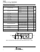
TERMINAL
TYPE
DESCRIPTION
NAME NO.
TYPE
DESCRIPTION
V
DD
1, 9,
23, 38,
48
Supply Digital logic power. Provides power for all digital circuitry and digital I/O buffers.
V
DDA
55, 57 Supply Analog power. VDDA provides a supply reference for the high-speed analog circuits, receiver and
transmitter
GNDA 52, 58,
61
Ground Analog ground. GNDA provides a ground reference for the high-speed analog circuits, RX and TX.
GND 5, 13,
18, 28,
33, 43
Ground Digital logic ground. Provides a ground for the logic circuits and digital I/O buffers.
absolute maximum ratings over operating free-air temperature (unless otherwise noted)
†
Supply voltage, V
DD
(see Note 1) −0.3 V to 3 V. . . . . . . . . . . . . . . . . . . . . . . . . . . . . . . . . . . . . . . . . . . . . . . . . . . . .
Voltage range at TXD, ENABLE, GTX_CLK, TX_EN, TX_ER, LOOPEN, PRBS_PASS −0.3 V to 4 V. . . . . . . .
Voltage range at any other terminal except above −0.3 V to V
DD
+ 0.3 V. . . . . . . . . . . . . . . . . . . . . . . . . . . . . . . .
Package power dissipation, P
D
See Dissipation Rating Table. . . . . . . . . . . . . . . . . . . . . . . . . . . . . . . . . . . . . . . . .
Storage temperature, T
stg
−65°C to 150°C. . . . . . . . . . . . . . . . . . . . . . . . . . . . . . . . . . . . . . . . . . . . . . . . . . . . . . . . . .
Electrostatic discharge HBM:3 kV, CDM: 1.5 kV. . . . . . . . . . . . . . . . . . . . . . . . . . . . . . . . . . . . . . . . . . . . . . . . . . . . .
Characterized free-air operating temperature range, T
A
−40°C to 85°C. . . . . . . . . . . . . . . . . . . . . . . . . . . . . . . . . .
Lead temperature 1,6 mm (1/16 inch) from case for 10 seconds 260°C. . . . . . . . . . . . . . . . . . . . . . . . . . . . . . . . .
†
Stresses beyond those listed under “absolute maximum ratings” may cause permanent damage to the device. These are stress ratings only, and
functional operation of the device at these or any other conditions beyond those indicated under “recommended operating conditions” is not
implied. Exposure to absolute-maximum-rated conditions for extended periods may affect device reliability.
NOTE 1: All voltage values, except differential I/O bus voltages, are with respect to network ground.
DISSIPATION RATING TABLE
PACKAGE
T
A
≤ 25°C
POWER RATING
OPERATING FACTOR
‡
ABOVE T
A
= 25°C
T
A
= 70°C
POWER RATING
RCP64
§
5.25 W 46.58 mW/°C 2.89 W
RCP64
¶
3.17 W 23.70 mW/°C 1.74 W
RCP64
#
2.01 W 13.19 mW/°C 1.11 W
‡
This is the inverse of the traditional junction-to-ambient thermal resistance (R
θ
JA
).
§
2 oz. Trace and copper pad with solder
¶
2 oz. Trace and copper pad without solder
#
Standard JEDEC high-K board
For more information, refer to TI application note PowerPAD Thermally Enhanced Package, TI
literature number SLMA002