
Datasheet


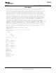


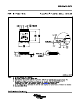
Table Of Contents

3.4
5
TSSOP
14-PinPWPPackage
2 3
´
0.1 Fm
0.1 Fm
33pF
0.1 Fm0.1 Fm 6.8 Fm
33pF
1kW 1kW
24.9 W
49.9 W49.9 W
24.9 W
THS7530
V
OUT+
V
OUT-
V
IN
V
S-
V
G-
V
CL-
V
CL+
V
OCM
V
G+
V
S+
=5V
PD
0.1 Fm
33pF
0.1 Fm0.1 Fm 6.8 Fm
33pF
1kW 1kW
24.9 W
24.9 W24.9 W
24.9 W
THS7530
V
OUT+
V
IN-
V
OUT-
V
IN+
V
S-
V
G-
V
CL-
V
CL+
V
OCM
V
G+
V
S+
=5V
PD
H
PD
THS7530
x1
V
CL+
V
S+
V
OUT+
V
OUT-
V
OCM
V
OCM
Error
Amplifier
V
CL-
V
S-
Output
Buffer
V
IN-
V
G-
V
IN+
V
G+
Power
Control
THS7530
SLOS405C –DECEMBER 2002–REVISED FEBRUARY 2010
www.ti.com
Figure 25. Recommended Thermal Land Size and
Thermal Via Patterns (Dimensions in mm)
Figure 23. DC-Coupled Single-Ended Input with
DC-Coupled Differential Output
See TI's Technical Brief titled, PowerPAD™
Thermally Enhanced Package (SLMA002) for a
detailed discussion of the PowerPAD™ package, its
dimensions, and recommended use.
THEORY OF OPERATION
Figure 26 shows a simplified schematic of the
THS7530.
The input architecture is a modified Gilbert cell. The
output from the Gilbert cell is converted to a voltage
and buffered to the output as a fully-differential signal.
A summing node between the outputs is used to
compare the output common-mode voltage to the
Figure 24. DC-Coupled Differential Input with
V
OCM
input. The V
OCM
error amplifier then servos the
DC-Coupled Differential Output
output common-mode voltage to maintain it equal to
the V
OCM
input. Left unterminated, V
OCM
is set to
midsupply by internal resistors.
LAYOUT CONSIDERATIONS
The gain control input is conditioned to give
The THS7530 comes in a thermally-enhanced
linear-in-dB gain control (block H). The gain control
PowerPAD™ package. Figure 25 shows the
input is a differential signal from 0 V to 0.9 V which
recommended number of vias and thermal land size
varies the gain from 11.6 dB to 46.5 dB.
recommended for best performance. Thermal vias
connect the thermal land to internal or external
V
CL+
and V
CL–
provide inputs that limit the output
copper planes and should have a drill diameter
voltage swing of the amplifier.
sufficiently small so that the via hole is effectively
plugged when the barrel of the via is plated with
copper. This plug is needed to prevent wicking the
solder away from the interface between the package
body and the thermal land on the surface of the
board during solder reflow. The experiments
conducted jointly with Solectron Texas indicate that a
via drill diameter of 0,33 mm (13 mils, or .013 in) or
smaller works well when 1-ounce copper is plated at
the surface of the board and simultaneously plating
the barrel of the via. If the thermal vias are not
plugged when the copper plating is performed, then a
solder mask material should be used to cap the vias
with a dimension equal to the via diameter + 0,1 mm
minimum. This prevents the solder from being wicked
through the thermal via and potentially creating a
solder void in the region between the package bottom
and the thermal land on the surface of the PCB.
Figure 26. THS7530 Simplified Schematic
12 Submit Documentation Feedback Copyright © 2002–2010, Texas Instruments Incorporated
Product Folder Link(s): THS7530