
Datasheet


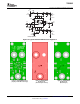

Table Of Contents
- FEATURES
- APPLICATIONS
- DESCRIPTION
- ABSOLUTE MAXIMUM RATING
- RECOMMENDED OPERATING CONDITIONS
- PACKAGE DISSIPATION RATINGS
- PIN ASSIGNMENTS
- ELECTRICAL CHARACTERISTICS
- TYPICAL CHARACTERISTICS
- TYPICAL THS4302 CHARACTERISTICS (5 V)
- TYPICAL THS4302 CHARACTERISTICS (3 V)
- APPLICATION INFORMATION
- ADDITIONAL REFERENCE MATERIAL

www.ti.com
APPLICATION INFORMATION
High-Speed Operational amplifiers
Applications Section Contents
_
+
THS4302
R
f
100 Ω
49.9 Ω
V
I
+
22 µF 47 pF 0.1 µF
V
S+
50-Ω Source
R
g
V
O
+ 22 µF 47 pF 0.1 µF
V
S−
30.1 Ω
30.1 Ω
FB
FB
FB = Ferrite Bead
THS4302
SLOS403H – OCTOBER 2002 – REVISED AUGUST 2006
generator. The 50- Ω series resistor at the V
O
terminal
in addition to the 50- Ω load impedance of the test
equipment, provides a 100- Ω load. The total 100- Ω
The THS4302 fixed-gain operational amplifier set new
load at the output, combined with the 250- Ω total
performance levels, combining low distortion, high
feedback network load, presents the THS4302 with
slew rates, low noise, and a gain bandwidth in excess
an effective output load of 71 Ω for the circuit of
of 2 GHz. To achieve the full performance of the
Figure 44 .
amplifier, careful attention must be paid to
printed-circuit board layout and component selection.
INTERNAL FIXED RESISTOR VALUES
In addition, the devices provide a power-down mode
DEVICE GAIN (V/V) R
f
R
g
with the ability to save power when the amplifier is
THS4302 +5 200 50
inactive.
• Wideband, Noninverting Operation
• Single Supply Operation
• Saving Power With Power-Down Functionality
• Driving an ADC With the THS4302
• Driving Capacitive Loads
• Power Supply Decoupling Techniques and
Recommendations
• Board Layout
• Printed-Circuit Board Layout Techniques for
Optimal Performance
• PowerPAD Design Considerations
• PowerPAD PCB Layout Considerations
• Thermal Analysis
• Design Tools
• Evaluation Fixtures and Application Support
Information
• Additional Reference Material
Figure 44. Wideband, Noninverting
Gain Configuration
• Mechanical Package Drawings
WIDEBAND, NONINVERTING OPERATION
SINGLE SUPPLY OPERATION
The THS4302 is a fixed-gain voltage feedback
The THS4302 is designed to operate from a single
operational amplifier, with power-down capability,
3-V to 5-V power supply. When operating from a
designed to operate from a single 3-V to 5-V power
single power supply, care must be taken to ensure
supply.
the input signal and amplifier are biased appropriately
to allow for the maximum output voltage swing. The
Figure 44 is the noninverting gain configuration used
circuits shown in Figure 45 demonstrate methods to
to demonstrate the typical performance curves. Most
configure an amplifier in a manner conducive for
of the curves were characterized using signal sources
single supply operation.
with 50- Ω source impedance, and with measurement
equipment presenting a 50- Ω load impedance. In
Figure 44 , the 49.9- Ω shunt resistor at the V
IN
terminal matches the source impedance of the test
12 Submit Documentation Feedback Copyright © 2002 – 2006, Texas Instruments Incorporated
Product Folder Link(s): THS4302