
Datasheet


OPA551, OPA552
13
SBOS100A
www.ti.com
INPUT PROTECTION
The OPA551 and OPA552 feature internal clamp diodes
to protect the inputs when voltages beyond the supply rails
are encountered. However, input current should be limited
to 5mA. In some cases, an external series resistor may be
required. Many input signals are inherently current-limtied,
therefore, a limiting resistor may not be required. Please
consider that a “large” series resistor, in conjunction with
the input capacitance, can affect stability.
USING THE OPA552 IN LOW GAINS
The OPA552 family is intended for applications with
signal gains of 5 or greater, but it is possible to take
advantage of their high slew rate in lower gains using an
external compensation technique in an inverting configu-
ration. This technique maintains low noise characteristics
of the OPA552 architecture at low frequencies. Depending
on the application, a small increase in high frequency
noise may result. This technique shapes the loop gain for
good stability while giving an easily controlled second-
order low-pass frequency response.
Considering only the noise gain (non-inverting signal
gain) for the circuit of Figure 11, the low frequency noise
gain (NG
1
) will be set by the resistor ratios, while the high
frequency noise gain (NG
2
) will be set by the capacitor
ratios. The capacitor values set both the transition fre-
quencies and the high frequency noise gain. If this noise
gain, determined by NG
2
= 1 + C
S
/C
F
, is set to a value
greater than the recommended minimum stable gain for
the op amp and the noise gain pole, set by 1/R
F
C
F
, is
placed correctly, a very well controlled, 2nd-order low-
pass frequency response will result.
To choose the values for both C
S
and C
F
, two parameters
and only three equations need to be solved. First, the
target for the high frequency noise gain (NG
2
) should be
greater than the minimum stable gain for the OPA552. In
the circuit in Figure 11, a target NG
2
of 10 is used.
Second, the signal gain of –1 shown in Figure 11 sets the
low frequency noise gain to NG
1
= 1 + R
F
/R
G
(=2 in this
example). Using these two gains, knowing the Gain Band-
width Product (GBP) for the OPA552 (12MHz), and
targeting a maximally flat 2nd-order, low-pass Butterworth
frequency response (Q = 0.707), the key frequency in the
compensation can be found.
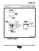
For the values shown in Figure 11, the f
–3dB
will be
approximately 956kHz. This is less than that predicted by
simply dividing the GBP by NG
1
. The compensation
network controls the bandwidth to a lower value while
providing the full slew rate at the output and an excep-
tional distortion performance due to increased loop gain at
frequencies below NG
1
• Z
0
. The capacitor values shown
in Figure 11 are calculated for NG
1
= 2 and NG
2
= 10 with
no adjustment for parasitics.
Actual circuit values can be optimized by check the
small-signal step response with actual load conditions.
Figure 12 shows the small-signal step response of this
OPA552, G = –1 circuit with a 500pF load. It is well-
behaved with no tendency to oscillate. If C
S
and C
F
were
removed, the circuit would be unstable.
FIGURE 11. Compensation of the OPA552 for G = 1.
FIGURE 12. Small-Signal Step Response for Figure 11.
SMALL-SIGNAL STEP RESPONSE
OPA552, G = –1, C
L
= 500pF
Time (1µs/div)
20mV/div
R
F
1kΩ
C
S
1.88nF
NG
1
= 1 + R
F
/R
G
= 2
NG
2
= 1 + C
S
/C
F
= 10
OPA552
+30V
–30V
V
IN
V
OUT
C
F
208pF
R
G
1kΩ
OPA552