
Datasheet


OPA547
11
SBOS056F
www.ti.com
Output Disable and Thermal Shutdown Status
As mentioned earlier, the OPA547’s output can be disabled
and the disable status can be monitored simultaneously.
Figures 9 and 10 provide examples using a single supply and
dual supplies, respectively.
OPA547
V+
E/S
Open Drain
(Output Disable)
HCT
(Thermal Status
Shutdown)
V–
FIGURE 9. Output Disable and Thermal Shutdown Status with
a Single Supply.
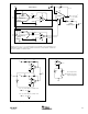
OUTPUT PROTECTION
Reactive and EMF-generating loads can return load cur-
rent to the amplifier, causing the output voltage to exceed
the power-supply voltage. This damaging condition can be
avoided with clamp diodes from the output terminal to the
power supplies, as shown in Figure 11. Schottkey rectifier
diodes with a 1A or greater continuous rating are recom-
mended.
FIGURE 10. Output Disable and Thermal Shutdown Status with Dual Supplies.
FIGURE 11. Motor Drive Circuit.
G = – = –4
R
2
R
1
3Ω
(Carbon)
0.01µF
R
2
20kΩ
R
1
5kΩ
OPA547
V–
V+
V
IN
Motor
D
1
D
2
D
1
, D
2
: International Rectifier 11DQ06.
OPA547
V+
E/S
NOTE: (1) Optional—may be required to limit leakage
current of optocoupler at high temperatures.
V–
(1)
6
1
2
4N38
Optocoupler
5
4
HCT or TTL In
5V
6
2
1
4N38
Optocoupler
5
4
Zetex
ZVN3310
TTL Out
7.5kΩ
1W
5V
OUTPUT STAGE COMPENSATION
The complex load impedances common in power op amp
applications can cause output stage instability. For normal
operation output compensation circuitry is not typically re-
quired. However, if the OPA547 is intended to be driven into
current limit, a R/C network may be required. Figure 11
shows an output series R/C compensation (snubber) net-
work (3Ω in series with 0.01µF) which generally provides
excellent stability. Some variations in circuit values may be
required with certain loads.