
Datasheet


ACLK
SMCLK
SMCLK
00
01
10
11
UCSSELx
UC1CLK
Prescaler/Divider
Bit Clock Generator
UCxBRx
16
BRCLK
Slave Address UC1SA
Transmit Shift Register
UCMST
Transmit Buffer UC 1TXBUF
I2C State Machine
Own Address UC1OA
Receive Shift Register
UCA10
Receive Buffer UC1RXBUF
UCGCEN
UCxSDA
UCxSCL
UCSLA10
www.ti.com
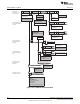
USCI Operation: I
2
C Mode
Figure 17-1. USCI Block Diagram: I
2
C Mode
17.3 USCI Operation: I
2
C Mode
The I
2
C mode supports any slave or master I
2
C-compatible device. Figure 17-2 shows an example of an
I
2
C bus. Each I
2
C device is recognized by a unique address and can operate as either a transmitter or a
receiver. A device connected to the I
2
C bus can be considered as the master or the slave when
performing data transfers. A master initiates a data transfer and generates the clock signal SCL. Any
device addressed by a master is considered a slave.
I
2
C data is communicated using the serial data pin (SDA) and the serial clock pin (SCL). Both SDA and
SCL are bidirectional, and must be connected to a positive supply voltage using a pullup resistor.
NOTE: SDA and SCL Levels
The MSP430 SDA and SCL pins must not be pulled up above the MSP430 V
CC
level.
451
SLAU144J–December 2004–Revised July 2013
Universal Serial Communication Interface, I
2
C Mode
Submit Documentation Feedback
Copyright © 2004–2013, Texas Instruments Incorporated