
Datasheet


R
T
Input
Voltage
STOP
RUN
LM5085
RT
VIN
R
T
=
V
OUT
x 6.67 x 10
6
F
S
- 33.4
R
T
=
V
OUT
x 6 x 10
6
F
S
- 8.6
R
T
=
V
OUT
x (V
IN
- 1.56V)
1.45 x 10
-7
x V
IN
x F
S
- 1.4
t
D
x (V
IN
- 1.56V)
1.45 x 10
-7
-
F
S
=
V
OUT
x (V
IN
- 1.56V + R
T
/3167)
V
IN
x [(1.45 x 10
-7
x (R
T
+ 1.4)) + (t
D
x (V
IN
- 1.56V + R
T
/3167))]
t
ON
=
(V
IN
- 1.56V + R
T
/3167)
1.45 x 10
-7
x (R
T
+ 1.4)
+ 50 ns
LM5085, LM5085-Q1
www.ti.com
SNVS565G –NOVEMBER 2008–REVISED MARCH 2013
ON-TIME TIMER
The on-time of the PFET gate drive output (PGATE pin) is determined by the resistor (R
T
) and the input voltage
(V
IN
), and is calculated from:
(3)
where R
T
is in kΩ.
The minimum on-time, which occurs at maximum V
IN
, should not be set less than 150ns (see Current Limiting
section). The buck regulator effective on-time, measured at the SW node (junction of Q1, L1, and D1) is typically
longer than that calculated in Equation 3 due to the asymmetric delay of the PFET. The on-time difference
caused by the PFET switching delay can be estimated as the difference of the turn-off and turn-on delays listed
in the PFET data sheet. Measuring the difference between the on-time at the PGATE pin versus the SW node in
the actual application circuit is also recommended.
In continuous conduction mode, the inverse relationship of t
ON
with V
IN
results in a nearly constant switching
frequency as V
IN
is varied. The operating frequency can be calculated from:
(4)
where R
T
is in kΩ, and t
D
is equal to 50ns plus the PFET’s delay difference. To set a specific continuous
conduction mode switching frequency (F
S
), the R
T
resistor is determined from the following:
(5)
where R
T
is in kΩ. A simplified version of Equation 5 at V
IN
= 12V, and t
D
= 100ns, is:
(6)
For V
IN
= 48V and t
D
= 100ns, the simplified equation is:
(7)
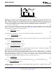
SHUTDOWN
The LM5085 can be shutdown by grounding the RT pin (see Figure 25). In this mode the PFET is held off, and
the VCC regulator is disabled. The internal operating current is reduced to the value shown in the graph
“Shutdown current vs. VIN”. The shutdown threshold at the RT pin is ≊0.73V, with ≊50mV of hysteresis.
Releasing the pin enables normal operation. The RT pin must not be forced high during normal operation.
Figure 25. Shutdown Implementation
Copyright © 2008–2013, Texas Instruments Incorporated Submit Documentation Feedback 11
Product Folder Links: LM5085 LM5085-Q1