
Datasheet


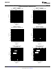


SDA
SCL
S
P
START condition
STOP condition
LM48100Q
SNAS470D –OCTOBER 2008–REVISED MARCH 2013
www.ti.com
APPLICATION INFORMATION
WRITE-ONLY I
2
C COMPATIBLE INTERFACE
The LM48100Q is controlled through an I
2
C compatible serial interface that consists of a serial data line (SDA)
and a serial clock (SCL). The clock line is uni-directional. The data line is bi-directional (open drain). The
LM48100Q and the master can communicate at clock rates up to 400kHz. Figure 14 shows the I
2
C interface
timing diagram. Data on the SDA line must be stable during the HIGH period of SCL. The LM48100Q is a
transmit/receive slave-only device, reliant upon the master to generate the SCL signal. Each transmission
sequence is framed by a START condition and a STOP condition (Figure 15). Each data word, device address
and data, transmitted over the bus is 8 bits long and is always followed by an acknowledge pulse (Figure 16).
The LM48100Q device address is 111110X, where X is determined by ADR (Table 2). ADR = 1 sets the device
address to 1111101. ADR = 0 sets the device address to 1111100.
I
2
C BUS FORMAT
The I
2
C bus format is shown in Figure 16. The START signal, the transition of SDA from HIGH to LOW while
SCL is HIGH, is generated, alerting all devices on the bus that a device address is being written to the bus.
The 7-bit device address is written to the bus, most significant bit (MSB) first, followed by the R/W bit. R/W = 0
indicates the master is writing to the slave device, RW = 1 indicates the master wants to read data from the slave
device. Set R/W = 0; the LM48100Q is a WRITE-ONLY device and will not respond the R/W = 1. The data is
latched in on the rising edge of the clock. Each address bit must be stable while SCL is HIGH. After the last
address bit is transmitted, the master device releases SDA, during which time, an acknowledge clock pulse is
generated by the slave device. If the LM48100Q receives the correct address, the device pulls the SDA line low,
generating an acknowledge bit (ACK).
Once the master device registers the ACK bit, the 8-bit register data word is sent. Each data bit should be stable
while SCL is HIGH. After the 8-bit register data word is sent, the LM48100Q sends another ACK bit. Following
the acknowledgement of the register data word, the master issues a STOP bit, allowing SDA to go high.
Figure 14. I
2
C Timing Diagram
Figure 15. Start and Stop Diagram
10 Submit Documentation Feedback Copyright © 2008–2013, Texas Instruments Incorporated
Product Folder Links: LM48100Q