
Datasheet


FB
SW
L1
LM34923
R3
C2
V
OUT
R
FB2
R
FB1
SW
FB
LM34923
L1
C2
CB
CA
RA
V
OUT
R
FB2
R
FB1
LM34923
www.ti.com
SNVS695A –MARCH 2011–REVISED FEBRUARY 2013
where t
ON
is the maximum on-time (at minimum input voltage), and ΔV is the desired ripple amplitude at the
RA/CA junction (typically 40-50 mV). RA and CA are then chosen from standard value components to satisfy the
above product. Typically CA is 1000 pF to 5000 pF, and RA is 10 kΩ to 300 kΩ. CB is then chosen large
compared to CA, typically 0.1 µF.
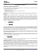
Figure 37. Minimum Output Ripple Using Ripple Injection
c) Alternate minimum ripple configuration: The circuit in Figure 38 is the same as that in the Block Diagram,
except the output voltage is taken from the junction of R3 and C2. The ripple at V
OUT
is determined by the
inductor’s ripple current and C2’s characteristics. However, R3 slightly degrades the load regulation. This circuit
may be suitable if the load current is fairly constant.
Figure 38. Alternate Minimum Output Ripple
PC Board Layout
The LM34923 regulation, over-voltage, and current limit comparators are very fast, and respond to short duration
noise pulses. Layout considerations are therefore critical for optimum performance. The layout must be as neat
and compact as possible, and all of the components must be as close as possible to the associated pins. The
two major current loops have currents which switch very fast, and so the loops should be as small as possible to
minimize conducted and radiated EMI. The first loop is formed by C1, through VIN to the SW pin, L1, C2, and
back to C1. The second loop is formed by L1, C2, D1, and back to L1. Since a current equal to the load current
switches between these two loops with each transition from on-time to off-time and back to on-time, it is
imperative that the ground end of C1 have a short and direct connection to D1’s anode, without going through
vias or a lengthy route. The power dissipation in the LM34923 can be approximated by determining the total
conversion loss (P
IN
– P
OUT
), and then subtracting the power losses in D1, and in the inductor. The power loss in
the diode is approximately:
P
D1
= I
OUT
x V
F
x (1–D) (22)
where V
F
is the diode’s forward voltage drop, and D is the on-time duty cycle.
P
L1
= I
OUT
2
x R
L
x 1.1 (23)
Copyright © 2011–2013, Texas Instruments Incorporated Submit Documentation Feedback 19
Product Folder Links: LM34923