Datasheet
Table Of Contents
- FEATURES
- Applications
- DESCRIPTION
- Absolute Maximum Ratings
- Electrical Characteristics
- Typical Performance Characteristics
- Block Diagram
- Theory of Operation
- Application Hints
- SELECTING THE EXTERNAL CAPACITORS
- SELECTING THE OUTPUT CAPACITOR
- SELECTING THE INPUT CAPACITOR
- FEED-FORWARD COMPENSATION
- SELECTING DIODES
- LAYOUT HINTS
- SETTING THE OUTPUT VOLTAGE
- SWITCHING FREQUENCY
- DUTY CYCLE
- INDUCTANCE VALUE
- MAXIMUM SWITCH CURRENT
- CALCULATING LOAD CURRENT
- DESIGN PARAMETERS VSW AND ISW
- THERMAL CONSIDERATIONS
- MINIMUM INDUCTANCE
- INDUCTOR SUPPLIERS
- SHUTDOWN PIN OPERATION
- Application Hints
- Revision History

formula: If power dissipation exceeds the maximum specified above, the internal thermal protection
LM2733
www.ti.com
SNVS209E –NOVEMBER 2002–REVISED APRIL 2013
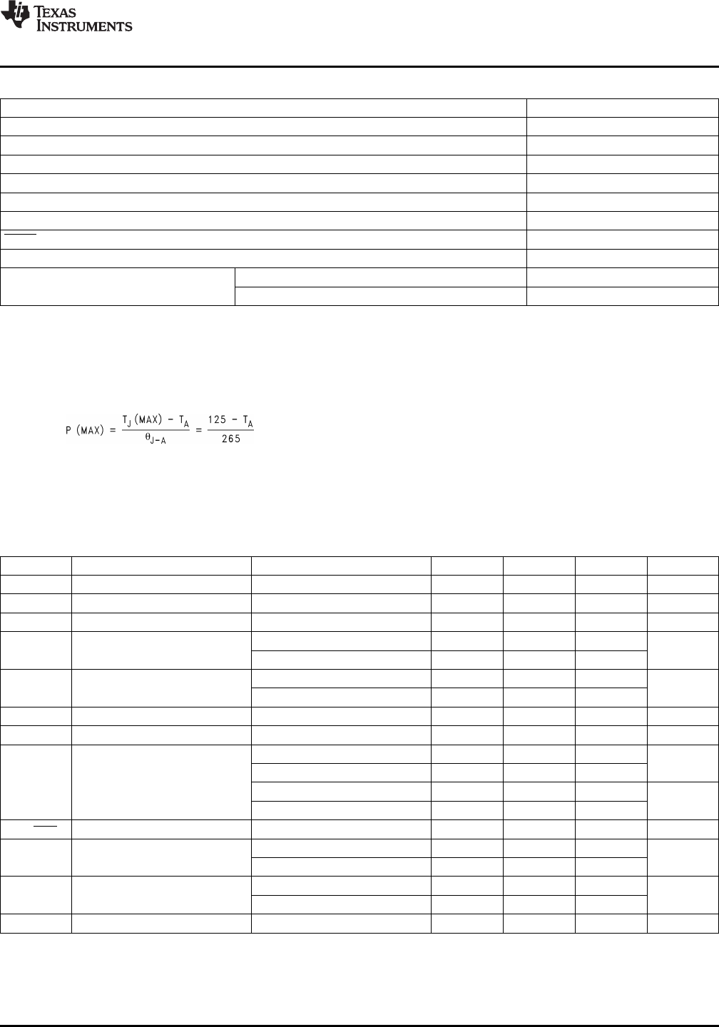
Absolute Maximum Ratings
(1)(2)
Storage Temperature Range −65°C to +150°C
Operating Junction Temperature Range −40°C to +125°C
Lead Temp. (Soldering, 5 sec.) 300°C
Power Dissipation
(3)
Internally Limited
FB Pin Voltage −0.4V to +6V
SW Pin Voltage −0.4V to +40V
Input Supply Voltage −0.4V to +14.5V
SHDN Pin Voltage −0.4V to VIN + 0.3V
θ
J-A
(SOT-23) 265°C/W
ESD Rating
(4)
Human Body Model 2 kV
Machine Model 200V
(1) Absolute Maximum Ratings indicate limits beyond which damage to the component may occur. Electrical specifications do not apply
when operating the device outside of the limits set forth under the operating ratings which specify the intended range of operating
conditions.
(2) If Military/Aerospace specified devices are required, please contact the Texas Instruments Sales Office/ Distributors for availability and
specifications.
(3) The maximum power dissipation which can be safely dissipated for any application is a function of the maximum junction temperature,
T
J
(MAX) = 125°C, the junction-to-ambient thermal resistance for the SOT-23 package, θ
J-A
= 265°C/W, and the ambient temperature,
T
A
. The maximum allowable power dissipation at any ambient temperature for designs using this device can be calculated using the
circuitry will protect the device by reducing the output voltage as required to maintain a safe junction temperature.
(4) The human body model is a 100 pF capacitor discharged through a 1.5 kΩ resistor into each pin. The machine model is a 200 pF
capacitor discharged directly into each pin.
Electrical Characteristics
Limits in standard typeface are for T
J
= 25°C, and limits in boldface type apply over the full operating temperature range
(−40°C ≤ T
J
≤ +125°C). Unless otherwise specified: V
IN
= 5V, V
SHDN
= 5V, I
L
= 0A.
Symbol Parameter Conditions Min
(1)
Typical
(2)
Max
(1)
Units
V
IN
Input Voltage 2.7 14 V
I
SW
Switch Current Limit See
(3)
1.0 1.5 A
R
DS
(ON) Switch ON Resistance I
SW
= 100 mA 500 650 mΩ
SHDN
TH
Shutdown Threshold Device ON 1.5
V
Device OFF 0.50
I
SHDN
Shutdown Pin Bias Current V
SHDN
= 0 0
µA
V
SHDN
= 5V 0 2
V
FB
Feedback Pin Reference Voltage V
IN
= 3V 1.205 1.230 1.255 V
I
FB
Feedback Pin Bias Current V
FB
= 1.23V 60 nA
I
Q
Quiescent Current V
SHDN
= 5V, Switching "X" 2.1 3.0
mA
V
SHDN
= 5V, Switching "Y" 1.1 2
V
SHDN
= 5V, Not Switching 400 500
µA
V
SHDN
= 0 0.024 1
Δ V
FB
ΔV
IN
FB Voltage Line Regulation 2.7V ≤ V
IN
≤ 14V 0.02 %/V
F
SW
Switching Frequency “X” Option 1.15 1.6 1.85
MHz
“Y” Option 0.40 0.60 0.8
D
MAX
Maximum Duty Cycle “X” Option 87 93
%
“Y” Option 93 96
I
L
Switch Leakage Not Switching V
SW
= 5V 1 µA
(1) Limits are specified by testing, statistical correlation, or design.
(2) Typical values are derived from the mean value of a large quantity of samples tested during characterization and represent the most
likely expected value of the parameter at room temperature.
(3) Switch current limit is dependent on duty cycle (see Typical Performance Characteristics). Limits shown are for duty cycles ≤ 50%.
Copyright © 2002–2013, Texas Instruments Incorporated Submit Documentation Feedback 3
Product Folder Links: LM2733


