
Datasheet


8
®
INA145
APPLICATION INFORMATION
The INA145 is a programmable gain difference amplifier
consisting of a gain of 1 difference amplifier and a program-
mable-gain output buffer stage. Basic circuit connections are
shown in Figure 1. Power supply bypass capacitors should
be connected close to pins 4 and 7, as shown. The amplifier
is programmable in the range of G = 1 to G = 1000 with two
external resistors.
The output of A1 is connected to the noninverting input of
A2 through a 10kΩ resistor which is trimmed to ±1%
absolute accuracy. The A2 input is available for applications
such as a filter or a precision current source. See application
figures for examples.
OPERATING VOLTAGE
The INA145 is fully specified for supply voltages from
±2.25V to ±18V, with key parameters guaranteed over the
temperature range –40°C to +85°C. The INA145 can be
operated with single or dual supplies, with excellent perfor-
mance. Parameters that vary significantly with operating
voltage, load conditions, or temperature are shown in the
typical performance curves.
SETTING THE GAIN
The gain of the INA145 is set by using two external
resistors, R
G1
and R
G2
, according to the equation:
G = 1 + R
G2
/R
G1
For a total gain of 1, A2 is connected as a buffer amplifier
with no R
G1
. A feedback resistor, R
G2
= 10kΩ, should be
used in the buffer connection. This provides bias current
cancellation (in combination with internal R
5
) to assure
specified offset voltage performance. Commonly used val-
ues are shown in the table of Figure 1. Resistor values for
other gains should be chosen to provide a 10kΩ parallel
resistance.
COMMON-MODE RANGE
The input resistors of the INA145 provides an input com-
mon-mode range that extends well beyond the power supply
rails. Exact range depends on the power supply voltage and
the voltage applied to the Ref terminal (pin 1). To assure
proper operation, the voltage at the non-inverting input of
A1 (an internal node) must be within its linear operating
range. Its voltage is determined by the simple 1:1 voltage
divider between pin 3 and pin 1. This voltage must be
between V– and (V+) – 1V.
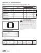
FIGURE 1. Basic Circuit Connections.
A1
V
IN
INA145
V
O
R
2
40kΩ
R
1
40kΩ
V
IN
R
3
40kΩ
R
4
40kΩ
R
G1
R
G2
R
B
A2
V
01
7
3
2
5
418
6
–V
S
+V
S
0.1µF
–
+
TOTAL GAIN
A2 GAIN
R
G1
R
G2
R
B
(V/V) (V/V) (W) (W) (W)
1 1 (None) 10k —
2 2 20k 20k —
5 5 12.4k 49.9k —
10 10 11.0k 100k —
20 20 10.5k 200k —
50 50 10.2k 499k —
100 100 10.2k 1M —
200 200 499 100k 9.53k
500 500 100 49.9k 10k
1000 1000 100 100k 10k
STANDARD 1% RESISTORS
0.1µF
V
O
= (V
IN
– V
IN
)(1 + R
G2
/R
G1
)
+–
R
5
10kΩ
(1%)