
Datasheet


www.ti.com
OUTPUT VOLTAGE STABILITY
APPLICATIONS
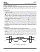
USING REF02 AS A POWER SUPPLY FOR THE DAC5571
REF02
15 V
5 V
1.14 mA
A0
SCL
SDA
I
2
C
Interface
V
OUT
= 0 V to 5 V
DAC5571
LAYOUT
DAC5571
SLAS405A – DECEMBER 2003 – REVISED AUGUST 2005
The DAC5571 exhibits excellent temperature stability of 5 ppm/ °C typical output voltage drift over the specified
temperature range of the device. This enables the output voltage to stay within a ±25- µV window for a ±1 °C
ambient temperature change. Combined with good dc noise performance and true 8-bit differential linearity, the
DAC5571 becomes a perfect choice for closed-loop control applications.
Due to the extremely low supply current required by the DAC5571, a possible configuration is to use a REF02
+5-V precision voltage reference to supply the required voltage to the DAC5571's supply input as well as the
reference input, as shown in Figure 47 . This is especially useful if the power supply is quite noisy or if the system
supply voltages are at some value other than 5 V. The REF02 outputs a steady supply voltage for the DAC5571.
If the REF02 is used, the current it needs to supply to the DAC5571 is 140 µA typical. When a DAC output is
loaded, the REF02 also needs to supply the current to the load. The total typical current required (with a 5-mW
load on a given DAC output) is: 140 µA + (5 mW/5 V) = 1.14 mA.
The load regulation of the REF02 is typically (0.005% ×V
DD
)/mA, which results in an error of 0.285 mV for the
1.14-mA current drawn from it. This corresponds to a 0.015 LSB error for a 0-V to 5-V output range.
Figure 47. REF02 as Power Supply to DAC5571
A precision analog component requires careful layout, adequate bypassing, and clean, well-regulated power
supplies.
The power applied to V
DD
should be well regulated and low noise. Switching power supplies and dc/dc
converters often has high-frequency glitches or spikes riding on the output voltage. In addition, digital
components can create similar high-frequency spikes as their internal logic switches states. This noise can easily
couple into the DAC output voltage through various paths between the power connections and analog output.
As with the GND connection, V
DD
should be connected to a +5-V power supply plane or trace that is separate
from the connection for digital logic until they are connected at the power entry point. In addition, the 1- µF to
10- µF and 0.1- µF bypass capacitors are strongly recommended. In some situations, additional bypassing may be
required, such as a 100- µF electrolytic capacitor or even a Pi filter made up of inductors and capacitors—all
designed to essentially low-pass filter the +5-V supply, removing the high-frequency noise.
18