
Datasheet


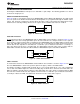


MSB
A1 A0 OP1 OP0 D7 D6 D5 D4 D3 D2 D1 D0 X X X X
DATA BITS
0 0 Write to specified register but do not update outputs.
0 1 Write to specified register and update outputs.
1 0 Write to all registers and update outputs.
1 1 Power-down outputs.
LSB
0 0 DAC A
0 1 DAC B
1 0 DAC C
1 1 DAC D
DAC084S085
www.ti.com
SNAS363E –MAY 2006–REVISED MARCH 2013
SERIAL INTERFACE
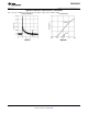
The three-wire interface is compatible with SPI™, QSPI and MICROWIRE, as well as most DSPs and operates
at clock rates up to 40 MHz. See the Timing Diagram for information on a write sequence.
A write sequence begins by bringing the SYNC line low. Once SYNC is low, the data on the D
IN
line is clocked
into the 16-bit serial input register on the falling edges of SCLK. To avoid misclocking data into the shift register,
it is critical that SYNC not be brought low simultaneously with a falling edge of SCLK (see Serial Timing Diagram,
Figure 2). On the 16th falling clock edge, the last data bit is clocked in and the programmed function (a change in
the DAC channel address, mode of operation and/or register contents) is executed. At this point the SYNC line
may be kept low or brought high. Any data and clock pusles after the 16th falling clock edge will be ignored. In
either case, SYNC must be brought high for the minimum specified time before the next write sequence is
initiated with a falling edge of SYNC.
Since the SYNC and D
IN
buffers draw more current when they are high, they should be idled low between write
sequences to minimize power consumption.
INPUT SHIFT REGISTER
The input shift register, Figure 30, has sixteen bits. The first two bits are address bits. They determine whether
the register data is for DAC A, DAC B, DAC C, or DAC D. The address bits are followed by two bits that
determine the mode of operation (writing to a DAC register without updating the outputs of all four DACs, writing
to a DAC register and updating the outputs of all four DACs, writing to the register of all four DACs and updating
their outputs, or powering down all four outputs). The final twelve bits of the shift register are the data bits. The
data format is straight binary (MSB first, LSB last), with all 0's corresponding to an output of 0V and all 1's
corresponding to a full-scale output of V
REFIN
- 1 LSB. The contents of the serial input register are transferred to
the DAC register on the sixteenth falling edge of SCLK. See Timing Diagram, Figure 2.
Figure 30. Input Register Contents
Normally, the SYNC line is kept low for at least 16 falling edges of SCLK and the DAC is updated on the 16th
SCLK falling edge. However, if SYNC is brought high before the 16th falling edge, the data transfer to the shift
register is aborted and the write sequence is invalid. Under this condition, the DAC register is not updated and
there is no change in the mode of operation or in the DAC output voltages.
POWER-ON RESET
The power-on reset circuit controls the output voltages of the four DACs during power-up. Upon application of
power, the DAC registers are filled with zeros and the output voltages are 0V. The outputs remain at 0V until a
valid write sequence is made to the DAC.
POWER-DOWN MODES
The DAC084S085 has four power-down modes, two of which are identical. In power-down mode, the supply
current drops to 20 µA at 3V and 30 µA at 5V. The DAC084S085 is set in power-down mode by setting OP1 and
OP0 to 11. Since this mode powers down all four DACs, the address bits, A1 and A0, are used to select different
output terminations for the DAC outputs. Setting A1 and A0 to 00 or 11 causes the outputs to be tri-stated (a high
impedance state). While setting A1 and A0 to 01 or 10 causes the outputs to be terminated by 2.5 kΩ or 100 kΩ
to ground respectively (see Table 1).
Copyright © 2006–2013, Texas Instruments Incorporated Submit Documentation Feedback 15
Product Folder Links: DAC084S085