
Datasheet


CMBuffer
Internal
Voltage
Reference
Input
Circuitry
IN
P
IN
N
V
CM
1.2kW
1.2kW
ADS528x
(2mA) f´
S
50MSPS
5nHto9nH(TQFP-80)
2nHto3nH(QFN-64)
1.5pF
to2.4pF
IN OUT
IN
P
1.5pFto
2.5pF
1W
1000W
to1440W
5W
to10W
1000W
to1440W
5nHto9nH(TQFP-80)
2nHto3nH(QFN-64)
IN
N
1.5pFto
2.5pF
1W
15W
to25W
15W
to30W
0.2pF
to0.3pF
IN OUT
1.5pF
to2.4pF
IN OUT
5W
to10W
15W
to25W
15W
to30W
IN OUT
IN
OUT
16 to32W W
IN OUT
IN OUT
OUT
P
OUT
N
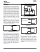
SwitchesthatareON
inSAMPLEphase.
SwitchesthatareON
inHOLDphase.
ADS5281
ADS5282
www.ti.com
SBAS397I –DECEMBER 2006–REVISED JUNE 2012
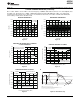
Figure 34. Analog Input Circuit Model
during ac-coupling by increasing V
CM
by roughly
Input Common-Mode Current
75mV. When operating above 50MSPS, it is
recommended that additional parallel resistors be
The input stage of all eight ADCs together sinks a
added externally to restore the input common-mode
common-mode current on the order of 2mA at
to at least 1.4V, if the inputs are to be ac-coupled.
50MSPS. Equation 3 describes the dependency of
the common-mode current and the sampling
frequency.
(3)
If the driving stage is dc-coupled to the inputs, then
Equation 3 can be used to determine its common-
mode drive capability and impedance. The inputs can
also be ac-coupled to the IN
N
and IN
P
pins. In that
case, the input common-mode is set by two internal
1.2kΩ resistors connecting the input pins to V
CM
. This
architecture is shown in Figure 35.
When the inputs are ac-coupled, there is a drop in
the voltages at IN
P
and IN
N
relative to V
CM
. This can
Dashed area denotes one of eight channels.
be computed from Equation 3. At 50MSPS, for
Figure 35. Common-Mode Biasing of Input Pins
example, the drop at each of the 16 input pins is
150mV, which is not optimal for ADC operation.
Initialization Registers 1 and 5, described in the
Initialization Registers table, can be used to partially
reduce the effect of this input common-mode drop
Copyright © 2006–2012, Texas Instruments Incorporated 33