
Datasheet


S
1
S
2
10pF
AINP
ADS1601
8pF
VMID
S
1
S
2
10pF
AINN
8pF
VMID
AGND
392W
OPA2822
ADS1601
AGND
OPA2822
40pF
V
CM
(1)
V
CM
(1)
V
CM
(1)
100pF
AINP
AINN
100pF
(3)
392W
40pF
100pF
(2)
(2)
(2)
(2)
392W
392W
392W
0.01 Fm
0.01 Fm
392W
1 Fm392W
1kW
1kW
1 Fm392W
49.9W
49.9W
-
V
IN
2
+V
CM
V
IN
2
+V
CM
On
S
1
S
2
Off
On
Off
t = f
SAMPLE CLK
1/
ADS1601
THS4503
22pF
-V
IN
+V
IN
100pF
100pF
AINP
AINN
100pF
24.9W
392W
392W
24.9W
392W
392W
22pF
V
CM
ADS1601
SBAS322D –DECEMBER 2004–REVISED OCTOBER 2011
www.ti.com
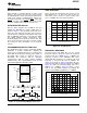
INPUT CIRCUITRY drivers close to the inputs and use good capacitor
bypass techniques on their supplies, such as a
The ADS1601 uses switched-capacitor circuitry to
smaller high-quality ceramic capacitor in parallel with
measure the input voltage. Internal capacitors are
a larger capacitor. Keep the resistances used in the
charged by the inputs and then discharged internally
driver circuits low—thermal noise in the driver circuits
with this cycle repeating at the frequency of CLK.
degrades the overall noise performance. When the
Figure 36 shows a conceptual diagram of these
signal can be ac-coupled to the ADS1601 inputs, a
circuits. Switches S
2
represent the net effect of the
simple RC filter can set the input common-mode
modulator circuitry in discharging the sampling
voltage. The ADS1601 is a high-speed,
capacitors; the actual implementation is different. The
high-performance ADC. Special care must be taken
timing for switches S
1
and S
2
is shown in Figure 37.
when selecting the test equipment and setup used
with this device. Pay particular attention to the signal
sources to ensure they do not limit performance when
measuring the ADS1601.
Figure 36. Conceptual Diagram of Internal
Circuitry Connected to the Analog Inputs
(1) Recommended V
CM
= 2.7V.
(2) Optional ac-coupling circuit provides common-mode input
voltage.
(3) Increase to 390pF when f
IN
≤ 100kHz for improved SNR and
THD.
Figure 38. Recommended Driver Circuit Using
the OPA2822
Figure 37. Timing for the Switches in Figure 36
DRIVING THE INPUTS
The external circuits driving the ADS1601 inputs must
be able to handle the load presented by the switching
capacitors within the ADS1601. The input switches S
1
in Figure 36 are closed for approximately one-half of
the sampling period, t
SAMPLE
, allowing only ≉ 24ns for
the internal capacitors to be charged by the inputs
when f
CLK
= 20MHz.
Figure 38 and Figure 39 show the recommended
circuits when using single-ended or differential op
amps, respectively. The analog inputs must be driven
Figure 39. Recommended Driver Circuit Using
differentially to achieve optimum performance. The
the THS4503 Differential Amplifier
external capacitors, between the inputs and from
each input to AGND, improve linearity and should be
placed as close to the pins as possible. Place the
16 Copyright © 2004–2011, Texas Instruments Incorporated