
Datasheet


VDD
GND
SCL
SDA
ADDR
A T
(ADS1014/5Only)
LER
AIN0
AIN1
AIN2(ADS1015Only)
AIN3(ADS1015Only)
SCL
SDA
1 F00n
I C-Capabl Mastere
( )MSP430
2
ADS1 13/4/0 5
+3.3V
VDD
GND
1 F00n
+3.3V
JTAG
Serial AR/U T
+3.3V
10kW 10kW
ADS1013
ADS1014
ADS1015
SBAS473C –MAY 2009–REVISED OCTOBER 2009
www.ti.com
QUICKSTART GUIDE For example, to write to the configuration register to
set the ADS1013/4/5 to continuous conversion mode
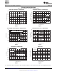
This section provides a brief example of ADS1013/4/5
and then read the conversion result, send the
communications. Refer to subsequent sections of this
following bytes in this order:
data sheet for more detailed explanations. Hardware
for this design includes: one ADS1013/4/5 configured Write to Config register:
with an I
2
C address of 1001000; a microcontroller
First byte: 0b10010000 (first 7-bit I
2
C address
with an I
2
C interface (TI recommends the MSP430
followed by a low read/write bit)
product line); discrete components such as resistors,
capacitors, and serial connectors; and a 2V to 5V
Second byte: 0b00000001 (points to Config register)
power supply. Figure 9 shows the basic hardware
Third byte: 0b00000100 (MSB of the Config register
configuration.
to be written)
The ADS1013/4/5 communicate with the master
Fourth byte: 0b10000011 (LSB of the Config register
(microcontroller) through an I
2
C interface. The master
to be written)
provides a clock signal on the SCL pin and data are
transferred via the SDA pin. The ADS1013/4/5 never
Write to Pointer register:
drive the SCL pin. For information on programming
First byte: 0b10010000 (first 7-bit I
2
C address
and debugging the microcontroller being used, refer
followed by a low read/write bit)
to the device-specific product data sheet.
Second byte: 0b00000000 (points to Conversion
The first byte sent by the master should be the
register)
ADS1013/4/5 address followed by a bit that instructs
the ADS1013/4/5 to listen for a subsequent byte. The
Read Conversion register:
second byte is the register pointer. Refer to Table 6
First byte: 0b10010001 (first 7-bit I
2
C address
for a register map. The third and fourth bytes sent
followed by a high read/write bit)
from the master are written to the register indicated in
the second byte. Refer to Figure 16 and Figure 17 for
Second byte: the ADS1013/4/5 response with the
read and write operation timing diagrams,
MSB of the Conversion register
respectively. All read and write transactions with the
Third byte: the ADS1013/4/5 response with the LSB
ADS1013/4/5 must be preceded by a start condition
of the Conversion register
and followed by a stop condition.
Figure 9. Basic Hardware Configuration
8 Submit Documentation Feedback Copyright © 2009, Texas Instruments Incorporated
Product Folder Link(s): ADS1013 ADS1014 ADS1015