
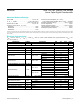
Datasheet


Note 5:
Drive HA with a 1kHz GND to V
DD
amplitude tone. LA = LB = GND. No load. WB is at midscale with a 10pF load. Measure WB.
Note 6: The wiper settling time is the worst-case 0 to 50% rise time, measured between tap 0 and tap 127. H_ = V
DD
, L_ = GND,
and the wiper terminal is loaded with 10pF capacitance to ground.
Note 7: Digital timing is guaranteed by design and characterization, not production tested.
Note 8: The SCL clock period includes rise and fall times (t
R
= t
F
). All digital input signals are specified with t
R
= t
F
= 2ns and timed
from a voltage level of (V
IL
+ V
IH
)/2.
(V
DD
= 5V, T
A
= +25°C, unless otherwise noted.)
Figure 1. Voltage-Divider and Variable Resistor Configurations
H
L
W W
N.C.
L
DIGITAL INPUT VOLTAGE (V)
SUPPLY CURRENT (µA)
4.54.03.53.02.52.01.51.00.5
1
10
100
1000
10,000
0.1
0 5.0
SUPPLY CURRENT
vs. DIGITAL INPUT VOLTAGE
MAX5387 toc02
V
DD
= 5V
V
DD
= 2.6V
SUPPLY CURRENT
vs. SUPPLY VOLTAGE
MAX5387 toc03
V
DD
(V)
I
DD
(μA)
0.1
0.2
0.3
0.4
0.5
0.6
0.7
0.8
0.9
1.0
0
5.14.64.13.63.12.6
RESISTANCE (W-TO-L)
vs. TAP POSITION (10k
Ω)
TAP POSITION
W-TO-L RESISTANCE (kΩ
)
25520415351 102
3
9
6
11
0
4
10
7
2
8
5
1
0
MAX5387 toc04
RESISTANCE (W-TO-L)
vs. TAP POSITION (50k
Ω)
TAP POSITION
W-TO-L RESISTANCE (kΩ)
25520415351 102
15
45
30
55
0
20
50
35
10
40
25
5
0
MAX5387 toc05
RESISTANCE (W-TO-L)
vs. TAP POSITION (100kΩ)
MAX5387 toc06
TAP POSITION
RESISTANCE (W-TO-L) (kΩ)
20415310251
10
20
30
40
50
60
70
80
90
100
110
0
0 255
SUPPLY CURRENT vs. TEMPERATURE
MAX5387 toc01
TEMPERATURE (°C)
SUPPLY CURRENT (μA)
1109565 80-10 5 20 35 50-25
0.1
0.2
0.3
0.4
0.5
0.6
0.7
0.8
0.9
1.0
0
-40 125
V
DD
= 5V
V
DD
= 2.6V
MAX5387 Dual, 256-Tap, Volatile, Low-Voltage
Linear Taper Digital Potentiometer
www.maximintegrated.com
Maxim Integrated
│
4
Typical Operating Characteristics
Electrical Characteristics (continued)