
Datasheet


MAX5062/MAX5063/MAX5064
Applications Information
Supply Bypassing and Grounding
Pay extra attention to bypassing and grounding the
MAX5062/MAX5063/MAX5064. Peak supply and output
currents may exceed 4A when both drivers are driving
large external capacitive loads in-phase. Supply drops
and ground shifts create forms of negative feedback for
inverters and may degrade the delay and transition
times. Ground shifts due to insufficient device ground-
ing may also disturb other circuits sharing the same AC
ground return path. Any series inductance in the V
DD
,
DH, DL, and/or GND paths can cause oscillations due
to the very high di/dt when switching the MAX5062/
MAX5063/MAX5064 with any capacitive load. Place
one or more 0.1µF ceramic capacitors in parallel as
close to the device as possible to bypass V
DD
to GND
(MAX5062/MAX5063) or PGND (MAX5064). Use a
ground plane to minimize ground return resistance and
series inductance. Place the external MOSFET as close
as possible to the MAX5062/MAX5063/MAX5064 to fur-
ther minimize board inductance and AC path resis-
tance. For the MAX5064_ the low-power logic ground
(AGND) is separated from the high-power driver return
(PGND). Apply the logic-input signal between IN_ to
AGND and connect the load (MOSFET gate) between
DL and PGND.
Power Dissipation
Power dissipation in the MAX5062/MAX5063/MAX5064
is primarily due to power loss in the internal boost
diode and the nMOS and pMOS FETS.
For capacitive loads, the total power dissipation for the
device is:
PCV f I I V
D L DD SW DDO BSTO DD
=× ×
⎛
⎝
⎞
⎠
++
()
×
2
125V/2A, High-Speed,
Half-Bridge MOSFET Drivers
12 ______________________________________________________________________________________
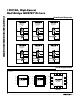
Figure 3. Minimum Pulse-Width Behavior for High Duty-Cycle Input (Off-Time < t
PW-MIN
)
PWM
IN
DH
DL
EXTERNAL
BBM DELAY
t
DMIN-DH-L
POTENTIAL
OVERLAP TIME
t
DMIN-DL-H
MAX5062B/MAX5062D/MAX5063B/MAX5063D/MAX5064
MAX5062A/MAX5062C/MAX5063A/MAX5063C/MAX5064
EXTERNAL
BBM DELAY
A)
B)
C)
N
N
PWM
IN
V
IN
V
OUT
INH
INL
DH
DL
HS
EXTERNAL
BBM DELAY
N
N
PWM
IN
V
IN
V
DD
V
DD
V
OUT
INH
INL
DH
DL
HS