
Datasheet


MAX381/MAX383/MAX385
Precision, Low-Voltage Analog Switches
_______________________________________________________________________________________ 3
ELECTRICAL CHARACTERISTICS—Dual Supplies (continued)
(V+ = +5V ±10%, V- = -5V ±10%, GND = 0V, V
INH
= 2.4V, V
INL
= 0.8V, T
A
= T
MIN
to T
MAX
, unless otherwise noted.)
PARAMETER SYMBOL
MIN TYP MAX
(Note 2)
UNITS
Input Current with Input
Voltage High
I
INH
-1.0 0.005 1.0 µA
CONDITIONS
V
IN
= 2.4V, all others = 0.8V
Input Current with Input
Voltage Low
I
INL
-1.0 0.005 1.0 µAV
IN
= 0.8V, all others = 2.4V
Turn-On Time t
ON
100 175
ns
Charge Injection
(Note 3)
V
CTE
25pC
C
L
= 1.0nF, V
GEN
= 0V,
R
GEN
= 0Ω, Figure 4
T
A
= +25°C
T
A
= T
MIN
to T
MAX
225
V
COM
= 3V, Figure 2
T
A
= +25°C
T
A
= T
MIN
to T
MAX
150
V
COM
= 3V, Figure 2Turn-Off Time t
OFF
60 100
ns
Power-Supply Range
MAX383 only, Figure 3
Break-Before-Make
Time Delay (Note 3)
t
D
10 20 ns
T
A
= +25°C
T
A
= +25°C
R
L
= 100Ω, C
L
= 5pF,
f = 1MHz, Figure 5
Off Isolation (Note 6) V
ISO
72 dB
T
A
= +25°C
R
L
= 50Ω, C
L
= 5pF,
f = 1MHz, Figure 6
Crosstalk (Note 7) V
CT
90 dB
T
A
= +25°Cf = 1MHz, Figure 7Off Capacitance C
OFF
12 pF
T
A
= +25°Cf = 1MHz, Figure 7COM Off Capacitance C
COM(OFF)
12 pF
T
A
= +25°Cf = 1MHz, Figure 8Channel On Capacitance C
COM(ON)
pF
±3 ±8 V
Positive Supply Current
39
I+
All channels on or off,
V+ = 5.5V, V- = -5.5V, V
IN
= 0V or V+
-1.0 0.06 1.0 µA
Negative Supply
Current
I-
All channels on or off,
V+ = 5.5V, V- = -5.5V, V
IN
= 0V or V+
-1.0 -0.01 1.0 µA
Logic High Input Voltage V
AH
2.4 V
Logic Low Input Voltage V
AL
0.8 VT
A
= T
MIN
to T
MAX
T
A
= T
MIN
to T
MAX
Note 2: The algebraic convention, where the most negative value is a minimum and the most positive value a maximum, is used in
this data sheet.
Note 3: Guaranteed by design.
Note 4: ∆R
ON
= ∆R
ON
(max) - ∆R
ON
(min). On-resistance match between channels and flatness are guaranteed only with
specified voltages. Flatness is defined as the difference between the maximum and minimum value of on-resistance as
measured over the specified analog signal range.
Note 5: Leakage parameters are 100% tested at maximum rated hot temperature and guaranteed by correlation at room temperature.
Note 6: See Figure 4. Off isolation = 20log
10
V
COM
/V
NC
or V
NO
, V
COM
= output, V
NC
or
NO
= input to off switch.
Note 7: Between any two switches. See Figure 5.
Note 8: Leakage testing at single supply is guaranteed by testing with dual supplies.
T
A
= +25°C
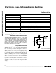
DIGITAL LOGIC INPUT
SUPPLY
DYNAMIC