
Datasheet


+3.3V, ±15kV ESD-Protected, Fail-Safe,
Hot-Swap, RS-485/RS-422 Transceivers
Pin Description
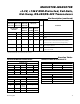
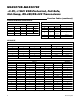
PIN
MAX3070E
MAX3073E
MAX3076E
MAX3071E
MAX3074E
MAX3077E
MAX3072E
MAX3075E
MAX3078E
MAX3079E
FULL-DUPLEX
DEVICES
HALF-
DUPLEX
DEVICES
FULL-
DUPLE
X MODE
HALF-
DUPLE
X MODE
NAME FUNCTION
— — — 1 1 H/F
Half-/Full-Duplex Select Pin. Connect H/F to V
CC
for half-
duplex mode; connect to GND or leave unconnected for
full-duplex mode.
2 2 1 2 2 RO
Receiver Output. When RE is low and if (A - B) -50mV,
RO is high; if (A - B) -200mV, RO is low.
3 — 2 3 3 RE
Receiver Output Enable. Drive RE low to enable RO; RO
is high impedance when RE is high. Drive RE high and
DE low to enter low-power shutdown mode. RE is a hot-
swap input (see the Hot-Swap Capability section for
details).
4 — 3 4 4 DE
Driver Output Enable. Drive DE high to enable driver
outputs. These outputs are high impedance when DE is
low. Drive RE high and DE low to enter low-power
shutdown mode. DE is a hot-swap input (see the Hot-
Swap Capability section for details).
5 3 4 5 5 DI
Driver Input. With DE high, a low on DI forces noninverting
output low and inverting output high. Similarly, a high on
DI forces noninverting output high and inverting output
low.
— — — 6 6 SRL
Slew-Rate Limit Selector Pin. Connect SRL to ground for
16Mbps communication rate; connect to V
CC
for
500kbps communication rate. Leave unconnected for
250kbps communication rate.
6, 7 4 5 7 7 GND Ground
— — — 8 8 TXP
Transmitter Phase. Connect TXP to ground or leave
unconnected for normal transmitter phase/polarity.
Connect to V
CC
to invert the transmitter phase/polarity.
9 5 — 9 — Y Noninverting Driver Output
— — — — 9 Y
Noninverting Driver Output and Noninverting Receiver
Input*
10 6 — 10 — Z Inverting Driver Output
— — — — 10 Z Inverting Driver Output and Inverting Receiver Input*
11 7 — 11 — B Inverting Receiver Input
— — — — 11 B Receiver Input Resistors*
— — 7 — — B Inverting Receiver Input and Inverting Driver Output
MAX3070E–MAX3079E
12
Maxim Integrated