
Datasheet


As the load current decreases, the modulator pole also
decreases; however, the modulator gain increases
accordingly, and the closed-loop unity-gain frequency
remains the same. Below is a numerical example to cal-
culate R
C
and C
C
values of the typical application cir-
cuit of Figure 4, where:
V
OUT
= 2.5V
I
OUT(MAX)
= 0.6A
C
OUT
= 10µF
R
ESR
= 0.010Ω
gm
EA
= 50µS
gm
C
= 2S
f
SWITCH
= 1.4MHz
R
LOAD
= V
OUT
/I
OUT(MAX)
= 2.5V/0.6A = 4.167Ω
fp
MOD
= 1/[2π C
OUT
(R
LOAD
+ R
ESR
)] = 1/[2π x
10 x 10
-6
(4.167 + 0.01)] = 3.80kHz.
fz
ESR
= 1/[2π C
OUT
R
ESR
] = 1/[2π x 10 x 10
-6
x
0.01] = 1.59MHz.
Pick a closed-loop unity-gain frequency (f
c
) of 50kHz.
The power modulator gain at fc is:
G
MOD
(fc) = gmc x R
LOAD
xfp
MOD
/f
c
= 2 x 4.167
x 3.80k/50k = 0.635
then:
R
C
= V
O
/(gm
EA
V
FB
G
MOD
(fc)) = 2.5/(50 x 10
-6
x
1.2 x 0.635) ≈ 62kΩ
C
C
= V
OUT
x(C
OUT
/R
C
) x I
OUT
(MAX) = 2.5 x 4.7
x 10
-6
/62k x 0.6 ≈ 680pF
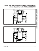
Applications Information
PCB Layout
Careful PCB layout is critical to achieve clean and sta-
ble operation. The switching power stage requires par-
ticular attention. Follow these guidelines for good PCB
layout:
1) Place decoupling capacitors as close to IC pins as
possible. Keep power ground plane (connected to
PGND) and signal ground plane (connected to
GND) separate. Connect the two ground planes
together with a single connection from PGND to
GND.
2) Input and output capacitors are connected to the
power ground plane; all other capacitors are con-
nected to signal ground plane.
3) Keep the high-current paths as short and wide as
possible.
4) If possible, connect IN, LX1, LX2, and PGND sepa-
rately to a large land area to help cool the IC to fur-
ther improve efficiency and long-term reliability.
5) Ensure all feedback connections are short and
direct. Place the feedback resistors as close to the
IC as possible.
6) Route high-speed switching nodes away from sen-
sitive analog areas (FB1, FB2, COMP1, COMP2).
MAX1970/MAX1971/MAX1972
Dual, 180° Out-of-Phase, 1.4MHz, 750mA Step-
Down Regulator with POR and RSI/PFO
______________________________________________________________________________________ 19