
Datasheet


MAX1822
4-Channel Load Switch with
No Pullup Resistors
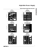
Multiple high-side switches can be driven from a single
MAX1822 high-side power supply with no pullup resis-
tors on the FET gates. In Figure 5, a MAX1822 supplies
high-side voltage to a MAX333 quad analog switch to
control any one of four high-side switches. The FET
gates are normally connected to ground when the
MAX333 logic inputs are low.
Low-Dropout Regulator
In Figure 6, a MAX1822 high-side power supply powers
an LM10 reference and op-amp combination, providing
sufficient gate drive to turn on the FET. This allows the
regulator to achieve less than 70mV dropout at 1A load
using an IRF541, and just under 20mV for a
SMP60N06.
The 200mV reference section is configured for a gain of
25 (e.g., 200mV x 25 = 5V) and connects to the nonin-
verting input of the op amp; the regulator’s output con-
nects directly to the inverting input. The op amp
amplifies the error between its inputs and varies the
gate drive to the FET, regulating the output. Capacitor
C6 reduces transients due to load changes; its size
depends on the magnitude of the load change in the
application and can be reduced or eliminated if the
load remains relatively constant. With C6 = 1000µF, the
output transient to a 1A load pulsed at 20Hz is typically
less than 150mV. The regulator is turned on by apply-
ing V
BATT
to the Enable/Shutdown input and turned off
by pulling this input to ground.
The regulator output voltage, V
OUT
, is set by the ratio of
R1 to R2, calculated as follows:
If the application does not require logic shutdown, con-
nect the MAX1822 V
CC
pin directly to the battery and
eliminate D2.
RR
V
OUT
21
02
1
.
=−
High-Side Power Supply
8 _______________________________________________________________________________________
Figure 5. MAX1822 Powering a MAX333 Quad Analog Switch, Realizing a 4-Channel Load Switch with No Pullup Resistors
MAX1822 MAX333
C1+
1
7
C1
0.01
µ
F
C4
1
µ
F
C3 10
µ
F
+3.5V TO +16.5V
C2
0.01
µ
F
6
2
4
5
8
C1-
C2+
4-CHANNEL LOAD SWITCH—NO PULLUP RESISTORS
C2-
GND
TO LOAD
ALL CAPACITORS = 1
µ
F (NOTE 2)
ALL TRANSISTORS = IRF541 (NOTE 1)
V
CC
V
OUT
TO LOAD
TO LOAD
TO LOAD
3
16
2
9
12
19
4
7
14
17
5
8
13
18
V-
IN1
SW1
SW2
SW3
SW4
1101120
IN2 IN3 IN4
NC4
NC3
NC1
N04
N03
N02
N01
V+
NC2
COM4
COM3
COM2
COM1
NOTE 1: TRANSISTOR TYPE DEPENDS
ON LOAD-CURRENT REQUIREMENTS.
NOTE 2: 1
µ
F CAPACITORS SUPRESS SWITCHING
TRANSIENTS—VALUE DEPENDS
ON LOAD CURRENT.