
Datasheet


MAX1620/MAX1621
Digitally Adjustable LCD Bias Supplies
______________________________________________________________________________________ 11
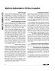
maximum switching frequency. The following equation
represents the output current for the ideal case (no
power losses) of Figure 5:
This means that a higher peak current is required to
achieve the same output current in the negative output
circuit as in the positive output circuit.
The output current for Figure 6 uses the same current
equation as the positive boost.
Output Voltage Control
The output voltage is set with a voltage divider to the
feedback pin (FB). For a positive output, the divider is
referred to GND; for a negative output, the divider is
referred to REF.
Output voltage can be adjusted with an internal DAC
summing current into FB through an external resistor.
The 5-bit DAC is controlled with a user-programmable
up/down counter. On power-up or after a reset, the
counter sets the DAC output to 10000 binary, or half-
scale.
I x (k-factor / L) x V / (V V )
OUT BATT BATT OUT
=+
1
2
2V
TO
15V
BATT
POK
N1
MMFT3055VL
V
DD
POL
SHDN (SUS)
DN (SDA)
UP (SCL)
REF
AGND
3
5
11
7
4
1
2
6
12
( ) ARE FOR MAX1621.
NOTE: CONNECTIONS TO DIGITAL INPUTS NOT SHOWN.
14
16
15
13
R3
300k
R4
300k
R5
1.2M
C6
100pF
10
9
8
LX
DHI
DLO
PGND
DOUT
FB
LCDON
3V
TO
5.5V
C1
0.1µF
C2
0.1µF
C3
22µF
C5
22µF
-6V
TO
-12V OUT
L1
100µH
D1
MBRS0540
D2
MBRS0540
C4
1µF
MAX1620
MAX1621
U1
R8
10k
TO REF
D3 1N6263 (ANY SCHOTTKY)
2V
TO
12V
BATT
POK
N1
MMFT3055VL
V
DD
POL
SHDN (SUS)
DN (SDA)
UP (SCL)
REF
AGND
3
5
11
7
4
1
2
6
12
( ) ARE FOR MAX1621.
NOTE: CONNECTIONS TO DIGITAL INPUTS NOT SHOWN.
14
16
15
13
R3
300k
R4
300k
R5
2.7M
C6
100pF
10
9
8
LX
DHI
DLO
PGND
DOUT
FB
LCDON
3V
TO
5.5V
C1
0.1µF
C2
0.1µF
C3
22µF
C5
22µF
-13.5V
TO
-27V OUT
L1
100µH
D2
MBRS0540
D1
MBRS0540
C4
2.2µF
MAX1620
MAX1621
U1
R8
10k
TO REF
D3 1N6263 (ANY SCHOTTKY)
Figure 5. Typical Operating Circuit—Negative Output
Figure 6. Alternative Negative Output—Maximum Voltage