
Datasheet


MAX1196
Dual 8-Bit, 40Msps, 3V, Low-Power ADC with
Internal Reference and Multiplexed Parallel Outputs
______________________________________________________________________________________ 15
Digital Output Data, Output Data Format
Selection (T/B), Output Enable (
OE
),
Channel Selection (A/B)
All digital outputs, D0A/B–D7A/B (CHA or CHB data) and
A/B are TTL/CMOS-logic compatible. The output coding
can be chosen to be either offset binary or two’s comple-
ment (Table 1) controlled by a single pin (T/B). Pull T/B
low to select offset binary and high to activate two’s com-
plement output coding. The capacitive load on the digital
outputs D0A/B–D7A/B should be kept as low as possible
(<15pF), to avoid large digital currents that could feed
back into the analog portion of the MAX1196, thereby
degrading its dynamic performance. Using buffers on
the digital outputs of the ADCs can further isolate the
digital outputs from heavy capacitive loads. To further
improve the dynamic performance of the MAX1196,
small-series resistors (e.g., 100Ω) can be added to the
digital output paths, close to the MAX1196.
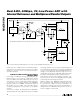
Figure 4 displays the timing relationship between out-
put enable and data output valid as well as power-
down/wake-up and data output valid.
Power-Down (PD) and Sleep
(SLEEP) Modes
The MAX1196 offers two power-save modes—sleep
and full power-down mode. In sleep mode (SLEEP = 1),
only the reference bias circuit is active (both ADCs are
disabled), and current consumption is reduced to 3mA.
To enter full power-down mode, pull PD high. With OE
simultaneously low, all outputs are latched at the last
value prior to the power down. Pulling OE high forces
the digital outputs into a high-impedance state.
Applications Information
Figure 5 depicts a typical application circuit containing
two single-ended-to-differential converters. The internal
reference provides a V
DD
/2 output voltage for level-shift-
ing purposes. The input is buffered and then split to a
voltage follower and inverter. One lowpass filter per
amplifier suppresses some of the wideband noise asso-
ciated with high-speed operational amplifiers. The user
can select the R
ISO
and C
IN
values to optimize the filter
performance, to suit a particular application. For the
application in Figure 5, an R
ISO
of 50Ω is placed before
the capacitive load to prevent ringing and oscillation.
The 22pF C
IN
capacitor acts as a small filter capacitor.
Using Transformer Coupling
An RF transformer (Figure 6) provides an excellent solu-
tion to convert a single-ended source signal to a fully dif-
ferential signal, required by the MAX1196 for optimum
performance. Connecting the center tap of the trans-
former to COM provides a V
DD
/2 DC level shift to the
input. Although a 1:1 transformer is shown, a step-up
transformer can be selected to reduce the drive require-
ments. A reduced signal swing from the input driver, such
as an op amp, can also improve the overall distortion.
DIFFERENTIAL INPUT
VOLTAGE*
DIFFERENTIAL INPUT
STRAIGHT OFFSET
BINARY
T/B = 0
TWO’S COMPLEMENT
T/B = 1
V
REF
× 255/256 +Full Scale - 1LSB 1111 1111 0111 1111
V
REF
× 1/256 +1LSB 1000 0001 0000 0001
0 Bipolar Zero 1000 0000 0000 0000
-V
REF
× 1/256 -1LSB 0111 1111 1111 1111
-V
REF
× 255/256 -Full Scale + 1LSB 0000 0001 1000 0001
-V
REF
× 256/256 -Full Scale 0000 0000 1000 0000
Table 1. MAX1196 Output Codes for Differential Inputs
*V
REF
= V
REFP
- V
REFN
OUTPUT
D0A/B–D7A/B
OE
t
DISABLE
t
ENABLE
HIGH-ZHIGH-Z
VALID DATA
Figure 4. Output Timing Diagram