
User's Manual


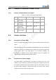


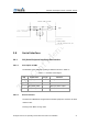
Table Of Contents
- Legal Information
- 1 About This Document
- 2 Product Overview
- 3 Interfaces
- 3.1 Definition of PINs
- 3.2 Working Condition
- 3.3 Feature of Interface Power Level
- 3.4 Power Interface
- 3.5 (U)SIM Card Interface
- 3.6 SD Card Interface
- 3.7 USB2.0 Interface
- 3.8 Serial Interface
- 3.9 JTAG (Joint Test Action Group) Interface
- 3.10 Power-on/Power-off & Reset Signal
- 3.11 Interactive Application Interface
- 3.12 LED Indicator Interface
- 4 Electric Feature
- 5 Technical Index of Radio Frequency
- 6 Related Test & Testing Standard
- 7 Design Guide
- 7.1 General Design Rule & Requirement
- 7.2 Power Supply Circuit Design
- 7.3 RF Circuit Design
- 7.4 Suggestions for EMC & ESD Design
- 7.5 Suggestions for PCB Wielding Panel Design
- 7.6 Suggestions for Heat-dissipation Design
- 7.7 Recommended Product Upgrading Plan
- 8 Manufacturing Guide
- 9 FCC Regulations:

Hardware Development Guide of Module Product
All Rights reserved, No Spreading abroad without Permission of ZTEWelink 21
Figure 3-4 USB Typical Circuit Application
3.8 Serial Interface
3.8.1 SPI (Serial Peripheral Interface) Bus Interface
3.8.1.1 Description of PINs
The definition of SPI interface signaling is defined as shown in Table 3-7.
Table 3-7 Definition of SPI Signal
PIN Signal Name I/O Type Function
39 SPI_ CS_N O SPI segment
40 SPI_ CLK O SPI clock
41 SPI_MISO_DATA B Main input, slave output
42 SPI_MOSI_DATA B Main input, slave output
3.8.1.2 Electric Feature
The SPI bus of ZM5202 is configured as the master equipment, and there are three
modes for SPI:
Running mode: Basic running mode.