
Micro Controller User's Manual


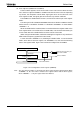


Table Of Contents
- TMP92CZ26AXBG
- 1. Outline and Features
- 2. Pin Assignment and Pin Functions
- 3. Operation
- 3.1 CPU
- 3.2 Memory Map
- 3.3 Clock Function and Standby Function
- 3.4 Boot ROM
- 3.5 Interrupts
- 3.6 DMAC (DMA Controller)
- 3.7 Function of ports
- 3.7.1 Port 1 (P10 to P17)
- 3.7.2 Port 4 (P40 to P47)
- 3.7.3 Port 5 (P50 to P57)
- 3.7.4 Port 6 (P60 to P67)
- 3.7.5 Port 7 (P70 to P76)
- 3.7.6 Port 8 (P80 to P87)
- 3.7.7 Port 9 (P90 to P92, P96, P97)
- 3.7.8 Port A (PA0 to PA7)
- 3.7.9 Port C (PC0 to PC7)
- 3.7.10 Port F (PF0 to PF5, PF7)
- 3.7.11 Port G (PG0 to PG5)
- 3.7.12 Port J (PJ0 to PJ7)
- 3.7.13 Port K (PK0 to PK7)
- 3.7.14 Port L (PL0 to PL7)
- 3.7.15 Port M (PM1, PM2, PM7)
- 3.7.16 Port N (PN0 to PN7)
- 3.7.17 Port P (PP1 to PP7)
- 3.7.18 Port R (R0 to R3)
- 3.7.19 Port T (PT0 to PT7)
- 3.7.20 Port U (PU0 to PU7)
- 3.7.21 Port V (PV0 to PV4, PV6, PV7)
- 3.7.22 Port W (PW0 to PW7)
- 3.7.23 Port X (PX4, PX5 and PX7)
- 3.7.24 Port Z (PZ0 to PZ7)
- 3.8 Memory Controller (MEMC)
- 3.9 External Memory Extension Function (MMU)
- 3.10 SDRAM Controller (SDRAMC)
- 3.11 NAND Flash Controller (NDFC)
- 3.11.1 Features
- 3.11.1 Block Diagram
- 3.11.2 Operation Description
- 3.11.3 ECC Control
- 3.11.4 Description of Registers
- 3.11.5 An Example of Accessing NAND Flash of SLC Type
- 3.11.6 An Example of Accessing NAND Flash of MLC Type (When the valid data is processed as 518byte)
- 3.11.7 An Example of Connections with NAND Flash
- 3.12 8 Bit Timer (TMRA)
- 3.13 16 bit timer / Event counter (TMRB)
- 3.14 Serial Channels (SIO)
- 3.15 Serial Bus Interface (SBI)
- 3.16 USB Controller
- 3.16.1 Outline
- 3.16.2 900/H1 CPU I/F
- 3.16.3 UDC CORE
- 3.16.3.1 SFRs
- 3.16.3.2 EPx_FIFO Register (x: 0 to 3)
- 3.16.3.3 bmRequestType Register
- 3.16.3.4 bRequest Register
- 3.16.3.5 wValue Register
- 3.16.3.6 wIndex Register
- 3.16.3.7 wLength Register
- 3.16.3.8 Setup Received Register
- 3.16.3.9 Current_Config Register
- 3.16.3.10 Standard Request Register
- 3.16.3.11 Request Register
- 3.16.3.12 DATASET Register
- 3.16.3.13 EPx_STATUS Register (x: 0 to 7)
- 3.16.3.14 EPx_SIZE Register (x: 0 to 7)
- 3.16.3.15 FRAME Register
- 3.16.3.16 ADDRESS Register
- 3.16.3.17 EOP Register
- 3.16.3.18 Port Status Register
- 3.16.3.19 Standard Request Mode Register
- 3.16.3.20 Request Mode Register
- 3.16.3.21 COMMAND Register
- 3.16.3.22 INT_Control Register
- 3.16.3.23 USB STATE Register
- 3.16.3.24 EPx_MODE Register (x: 1 to 3)
- 3.16.3.25 EPx_SINGLE Register
- 3.16.3.26 EPx_BCS Register
- 3.16.3.27 USBREADY Register
- 3.16.3.28 Set Descriptor STALL Register
- 3.16.3.29 Descriptor RAM Register
- 3.16.4 Descriptor RAM
- 3.16.5 Device Request
- 3.16.6 Transfer mode and Protocol Transaction
- 3.16.7 Bus Interface and Access to FIFO
- 3.16.8 USB Device answer
- 3.16.9 Power Management
- 3.16.10 Supplement
- 3.16.11 Points to Note and Restrictions
- 3.17 SPIC (SPI Controller)
- 3.18 I2S (Inter-IC Sound)
- 3.19 LCD Controller (LCDC)
- 3.20 Touch Screen Interface (TSI)
- 3.21 Real time clock (RTC)
- 3.22 Melody / Alarm generator (MLD)
- 3.23 Analog-Digital Converter (ADC)
- 3.23.1 Control register
- 3.23.2 Operation
- 3.23.2.1 Analog Reference Voltages
- 3.23.2.2 Analog Input Channel(s) selection
- 3.23.2.3 Starting an AD Conversion
- 3.23.2.4 AD Conversion Modes and AD Conversion-End Interrupts
- 3.23.2.5 High-Priority Conversion Mode
- 3.23.2.6 AD Monitor Function
- 3.23.2.7 AD Conversion Time
- 3.23.2.8 Storing and Reading the AD Conversion Result
- 3.23.2.9 Data Polling
- 3.24 Watchdog Timer (Runaway detection timer)
- 3.25 Power Management Circuit (PMC)
- 3.26 Multiply and Accumulate Calculation Unit (MAC)
- 3.27 Debug Mode
- 4. Electrical Characteristics
- 4.1 Maximum Ratings
- 4.2 DC Electrical Characteristics
- 4.3 AC Characteristics
- 4.3.1 Basic Bus Cycle
- 4.3.2 Page ROM Read Cycle
- 4.3.3 SDRAM controller AC Characteristics
- 4.3.4 NAND Flash Controller AC Characteristics
- 4.3.5 Serial channel timing
- 4.3.6 Timer input pulse (TA0IN, TA2IN, TB0IN0, TB1IN0)
- 4.3.7 Interrupt Operation
- 4.3.8 USB Timing (Full-speed)
- 4.3.9 LCD Controller
- 4.3.10 I2S Timing
- 4.3.11 SPI Controller
- 4.4 AD Conversion Characteristics
- 5. Table of Special function registers (SFRs)
- 6. Package

TMP92CZ26A
92CZ26A-277
TMRA23 Mode Register
7 6 5 4 3 2 1 0
Bit symbol TA23M1 TA23M0 PWM21 PWM20 TA3CLK1 TA3CLK0 TA2CLK1 TA2CLK0
Read/Write R/W
After reset 0 0 0 0 0 0 0 0
Function Operation mode
00: 8-bit timer mode
01: 16-bit timer mode
10: 8-bit PPG mode
11: 8-bit PWM mode
PWM cycle
00: Reserved
01: 2
6
10: 2
7
11: 2
8
TMRA3 clock for TMRA3
00: TA2TRG
01: φT1
10: φT16
11: φT256
TMRA2 clock for TMRA2
00: TA2IN pin
01: φT1
10: φT4
11: φT16
00 TA2IN (External input)
01 φT1
10 φT4
<TA2CLK1:0>
11 φT16
TA23MOD<TA23M1:0>≠01 TA23MOD<TA23M1:0>=01
00 Comparator output
from TMRA2
01 φT1
10 φT16
<TA3CLK1:0>
11 φT256
Overflow output from TMRA2
(16-bit timer mode)
00 Reserved
01 2
6
× Clock source
10 2
7
× Clock source
<PWM21:20>
11 2
8
× Clock source
00 8 timer × 2ch
01 16-bit timer
10 8-bit PPG
<TA23MA1:0>
11 8-bit PWM (TMRA2),
8-bit timer (TMRA3)
Figure 3.12.9 Register for TMRA (5)
TA23MOD
(110CH)
PWM c
y
cle selection
TMRA3 in
p
ut clock
TMRA23 o
p
eration mode selection
TMRA2 input clock