
Micro Controller User's Manual


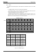


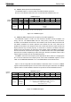


Table Of Contents
- TMP92CZ26AXBG
- 1. Outline and Features
- 2. Pin Assignment and Pin Functions
- 3. Operation
- 3.1 CPU
- 3.2 Memory Map
- 3.3 Clock Function and Standby Function
- 3.4 Boot ROM
- 3.5 Interrupts
- 3.6 DMAC (DMA Controller)
- 3.7 Function of ports
- 3.7.1 Port 1 (P10 to P17)
- 3.7.2 Port 4 (P40 to P47)
- 3.7.3 Port 5 (P50 to P57)
- 3.7.4 Port 6 (P60 to P67)
- 3.7.5 Port 7 (P70 to P76)
- 3.7.6 Port 8 (P80 to P87)
- 3.7.7 Port 9 (P90 to P92, P96, P97)
- 3.7.8 Port A (PA0 to PA7)
- 3.7.9 Port C (PC0 to PC7)
- 3.7.10 Port F (PF0 to PF5, PF7)
- 3.7.11 Port G (PG0 to PG5)
- 3.7.12 Port J (PJ0 to PJ7)
- 3.7.13 Port K (PK0 to PK7)
- 3.7.14 Port L (PL0 to PL7)
- 3.7.15 Port M (PM1, PM2, PM7)
- 3.7.16 Port N (PN0 to PN7)
- 3.7.17 Port P (PP1 to PP7)
- 3.7.18 Port R (R0 to R3)
- 3.7.19 Port T (PT0 to PT7)
- 3.7.20 Port U (PU0 to PU7)
- 3.7.21 Port V (PV0 to PV4, PV6, PV7)
- 3.7.22 Port W (PW0 to PW7)
- 3.7.23 Port X (PX4, PX5 and PX7)
- 3.7.24 Port Z (PZ0 to PZ7)
- 3.8 Memory Controller (MEMC)
- 3.9 External Memory Extension Function (MMU)
- 3.10 SDRAM Controller (SDRAMC)
- 3.11 NAND Flash Controller (NDFC)
- 3.11.1 Features
- 3.11.1 Block Diagram
- 3.11.2 Operation Description
- 3.11.3 ECC Control
- 3.11.4 Description of Registers
- 3.11.5 An Example of Accessing NAND Flash of SLC Type
- 3.11.6 An Example of Accessing NAND Flash of MLC Type (When the valid data is processed as 518byte)
- 3.11.7 An Example of Connections with NAND Flash
- 3.12 8 Bit Timer (TMRA)
- 3.13 16 bit timer / Event counter (TMRB)
- 3.14 Serial Channels (SIO)
- 3.15 Serial Bus Interface (SBI)
- 3.16 USB Controller
- 3.16.1 Outline
- 3.16.2 900/H1 CPU I/F
- 3.16.3 UDC CORE
- 3.16.3.1 SFRs
- 3.16.3.2 EPx_FIFO Register (x: 0 to 3)
- 3.16.3.3 bmRequestType Register
- 3.16.3.4 bRequest Register
- 3.16.3.5 wValue Register
- 3.16.3.6 wIndex Register
- 3.16.3.7 wLength Register
- 3.16.3.8 Setup Received Register
- 3.16.3.9 Current_Config Register
- 3.16.3.10 Standard Request Register
- 3.16.3.11 Request Register
- 3.16.3.12 DATASET Register
- 3.16.3.13 EPx_STATUS Register (x: 0 to 7)
- 3.16.3.14 EPx_SIZE Register (x: 0 to 7)
- 3.16.3.15 FRAME Register
- 3.16.3.16 ADDRESS Register
- 3.16.3.17 EOP Register
- 3.16.3.18 Port Status Register
- 3.16.3.19 Standard Request Mode Register
- 3.16.3.20 Request Mode Register
- 3.16.3.21 COMMAND Register
- 3.16.3.22 INT_Control Register
- 3.16.3.23 USB STATE Register
- 3.16.3.24 EPx_MODE Register (x: 1 to 3)
- 3.16.3.25 EPx_SINGLE Register
- 3.16.3.26 EPx_BCS Register
- 3.16.3.27 USBREADY Register
- 3.16.3.28 Set Descriptor STALL Register
- 3.16.3.29 Descriptor RAM Register
- 3.16.4 Descriptor RAM
- 3.16.5 Device Request
- 3.16.6 Transfer mode and Protocol Transaction
- 3.16.7 Bus Interface and Access to FIFO
- 3.16.8 USB Device answer
- 3.16.9 Power Management
- 3.16.10 Supplement
- 3.16.11 Points to Note and Restrictions
- 3.17 SPIC (SPI Controller)
- 3.18 I2S (Inter-IC Sound)
- 3.19 LCD Controller (LCDC)
- 3.20 Touch Screen Interface (TSI)
- 3.21 Real time clock (RTC)
- 3.22 Melody / Alarm generator (MLD)
- 3.23 Analog-Digital Converter (ADC)
- 3.23.1 Control register
- 3.23.2 Operation
- 3.23.2.1 Analog Reference Voltages
- 3.23.2.2 Analog Input Channel(s) selection
- 3.23.2.3 Starting an AD Conversion
- 3.23.2.4 AD Conversion Modes and AD Conversion-End Interrupts
- 3.23.2.5 High-Priority Conversion Mode
- 3.23.2.6 AD Monitor Function
- 3.23.2.7 AD Conversion Time
- 3.23.2.8 Storing and Reading the AD Conversion Result
- 3.23.2.9 Data Polling
- 3.24 Watchdog Timer (Runaway detection timer)
- 3.25 Power Management Circuit (PMC)
- 3.26 Multiply and Accumulate Calculation Unit (MAC)
- 3.27 Debug Mode
- 4. Electrical Characteristics
- 4.1 Maximum Ratings
- 4.2 DC Electrical Characteristics
- 4.3 AC Characteristics
- 4.3.1 Basic Bus Cycle
- 4.3.2 Page ROM Read Cycle
- 4.3.3 SDRAM controller AC Characteristics
- 4.3.4 NAND Flash Controller AC Characteristics
- 4.3.5 Serial channel timing
- 4.3.6 Timer input pulse (TA0IN, TA2IN, TB0IN0, TB1IN0)
- 4.3.7 Interrupt Operation
- 4.3.8 USB Timing (Full-speed)
- 4.3.9 LCD Controller
- 4.3.10 I2S Timing
- 4.3.11 SPI Controller
- 4.4 AD Conversion Characteristics
- 5. Table of Special function registers (SFRs)
- 6. Package

TMP92CZ26A
92CZ26A-97
ZZ12H
1234H
400001H
400000H
800000H
D15 ∼ D0
SRLLB
SRLUB
SRWR
RD
A23 ∼ A0
1CS
busak
busrq
int_xx
SDCLK
DMAC/read
DMAC/write
CPU execution
c
y
cle
Undefined after interrupt
request is asserted until
DMAC read cycle is
started
ZZ34H
CPU execution cycle
2CS
(2) Bus arbitration
The TMP92CZ26A includes three controllers (DMA controller, LCD controller, SDRAM
controller) that function as bus masters apart from the CPU. These controllers operate
independently and assert a bus request as required. The controller that receives a bus
acknowledgement acts as the bus master. No priorities are assigned to these three
controllers, and bus requests are processed in the order in which they are asserted. Once
one of the controllers owns the bus, bus requests from other controllers are put on hold until
the bus is released again. While one of the controllers is occupying the bus, CPU processing
including non-maskable interrupt requests is also put on hold.
(3) Transfer source and destination memory setting
Either internal or external memory can be set as the source and destination memory or
I/O to be accessed by the DMAC. Even when the MMU is used in external memory, the
addresses to be accessed by the DMAC should be specified using logical addresses. The
DMAC accesses the specified source and destination addresses according to the bus width
and number of waits set in the memory controller and the bank settings made in the MMU.
Although the bus sizing function is supported, the address alignment function is not
supported. Therefore, specify an even-numbered address for transferring 2 bytes and an
address that is an integral multiple of 4 for transferring 4 bytes.
Table 3.6.1 Difference point of address setting between HDMA and micro DMA
Data Length HDMA Micro DMA
1byte No restriction
2byte Even address
Source address
4byte Address in multiples of 4
1byte No restriction
2byte Even address
Destination address
4byte Address in multiples of 4
No restriction
(4) Operation timing
The following diagram shows an example of operation timing for transferring 2 bytes
from 16-bit memory connected with the
2CS area to 8-bit memory connected with the 1CS
area.