
Micro Controller User's Manual


Table Of Contents
- TMP92CZ26AXBG
- 1. Outline and Features
- 2. Pin Assignment and Pin Functions
- 3. Operation
- 3.1 CPU
- 3.2 Memory Map
- 3.3 Clock Function and Standby Function
- 3.4 Boot ROM
- 3.5 Interrupts
- 3.6 DMAC (DMA Controller)
- 3.7 Function of ports
- 3.7.1 Port 1 (P10 to P17)
- 3.7.2 Port 4 (P40 to P47)
- 3.7.3 Port 5 (P50 to P57)
- 3.7.4 Port 6 (P60 to P67)
- 3.7.5 Port 7 (P70 to P76)
- 3.7.6 Port 8 (P80 to P87)
- 3.7.7 Port 9 (P90 to P92, P96, P97)
- 3.7.8 Port A (PA0 to PA7)
- 3.7.9 Port C (PC0 to PC7)
- 3.7.10 Port F (PF0 to PF5, PF7)
- 3.7.11 Port G (PG0 to PG5)
- 3.7.12 Port J (PJ0 to PJ7)
- 3.7.13 Port K (PK0 to PK7)
- 3.7.14 Port L (PL0 to PL7)
- 3.7.15 Port M (PM1, PM2, PM7)
- 3.7.16 Port N (PN0 to PN7)
- 3.7.17 Port P (PP1 to PP7)
- 3.7.18 Port R (R0 to R3)
- 3.7.19 Port T (PT0 to PT7)
- 3.7.20 Port U (PU0 to PU7)
- 3.7.21 Port V (PV0 to PV4, PV6, PV7)
- 3.7.22 Port W (PW0 to PW7)
- 3.7.23 Port X (PX4, PX5 and PX7)
- 3.7.24 Port Z (PZ0 to PZ7)
- 3.8 Memory Controller (MEMC)
- 3.9 External Memory Extension Function (MMU)
- 3.10 SDRAM Controller (SDRAMC)
- 3.11 NAND Flash Controller (NDFC)
- 3.11.1 Features
- 3.11.1 Block Diagram
- 3.11.2 Operation Description
- 3.11.3 ECC Control
- 3.11.4 Description of Registers
- 3.11.5 An Example of Accessing NAND Flash of SLC Type
- 3.11.6 An Example of Accessing NAND Flash of MLC Type (When the valid data is processed as 518byte)
- 3.11.7 An Example of Connections with NAND Flash
- 3.12 8 Bit Timer (TMRA)
- 3.13 16 bit timer / Event counter (TMRB)
- 3.14 Serial Channels (SIO)
- 3.15 Serial Bus Interface (SBI)
- 3.16 USB Controller
- 3.16.1 Outline
- 3.16.2 900/H1 CPU I/F
- 3.16.3 UDC CORE
- 3.16.3.1 SFRs
- 3.16.3.2 EPx_FIFO Register (x: 0 to 3)
- 3.16.3.3 bmRequestType Register
- 3.16.3.4 bRequest Register
- 3.16.3.5 wValue Register
- 3.16.3.6 wIndex Register
- 3.16.3.7 wLength Register
- 3.16.3.8 Setup Received Register
- 3.16.3.9 Current_Config Register
- 3.16.3.10 Standard Request Register
- 3.16.3.11 Request Register
- 3.16.3.12 DATASET Register
- 3.16.3.13 EPx_STATUS Register (x: 0 to 7)
- 3.16.3.14 EPx_SIZE Register (x: 0 to 7)
- 3.16.3.15 FRAME Register
- 3.16.3.16 ADDRESS Register
- 3.16.3.17 EOP Register
- 3.16.3.18 Port Status Register
- 3.16.3.19 Standard Request Mode Register
- 3.16.3.20 Request Mode Register
- 3.16.3.21 COMMAND Register
- 3.16.3.22 INT_Control Register
- 3.16.3.23 USB STATE Register
- 3.16.3.24 EPx_MODE Register (x: 1 to 3)
- 3.16.3.25 EPx_SINGLE Register
- 3.16.3.26 EPx_BCS Register
- 3.16.3.27 USBREADY Register
- 3.16.3.28 Set Descriptor STALL Register
- 3.16.3.29 Descriptor RAM Register
- 3.16.4 Descriptor RAM
- 3.16.5 Device Request
- 3.16.6 Transfer mode and Protocol Transaction
- 3.16.7 Bus Interface and Access to FIFO
- 3.16.8 USB Device answer
- 3.16.9 Power Management
- 3.16.10 Supplement
- 3.16.11 Points to Note and Restrictions
- 3.17 SPIC (SPI Controller)
- 3.18 I2S (Inter-IC Sound)
- 3.19 LCD Controller (LCDC)
- 3.20 Touch Screen Interface (TSI)
- 3.21 Real time clock (RTC)
- 3.22 Melody / Alarm generator (MLD)
- 3.23 Analog-Digital Converter (ADC)
- 3.23.1 Control register
- 3.23.2 Operation
- 3.23.2.1 Analog Reference Voltages
- 3.23.2.2 Analog Input Channel(s) selection
- 3.23.2.3 Starting an AD Conversion
- 3.23.2.4 AD Conversion Modes and AD Conversion-End Interrupts
- 3.23.2.5 High-Priority Conversion Mode
- 3.23.2.6 AD Monitor Function
- 3.23.2.7 AD Conversion Time
- 3.23.2.8 Storing and Reading the AD Conversion Result
- 3.23.2.9 Data Polling
- 3.24 Watchdog Timer (Runaway detection timer)
- 3.25 Power Management Circuit (PMC)
- 3.26 Multiply and Accumulate Calculation Unit (MAC)
- 3.27 Debug Mode
- 4. Electrical Characteristics
- 4.1 Maximum Ratings
- 4.2 DC Electrical Characteristics
- 4.3 AC Characteristics
- 4.3.1 Basic Bus Cycle
- 4.3.2 Page ROM Read Cycle
- 4.3.3 SDRAM controller AC Characteristics
- 4.3.4 NAND Flash Controller AC Characteristics
- 4.3.5 Serial channel timing
- 4.3.6 Timer input pulse (TA0IN, TA2IN, TB0IN0, TB1IN0)
- 4.3.7 Interrupt Operation
- 4.3.8 USB Timing (Full-speed)
- 4.3.9 LCD Controller
- 4.3.10 I2S Timing
- 4.3.11 SPI Controller
- 4.4 AD Conversion Characteristics
- 5. Table of Special function registers (SFRs)
- 6. Package
TMP92CZ26A
92CZ26A-623
• Exiting the Power Cut Mode
The Power Cut Mode can be exited by external or internal interruption. (It inhibits to exit
the Power Cut Mode by reset when DVCC1A is cut off. Reset must be asserted after supplying
power to DVCC1A and waiting for its voltage to fully stabilize.) The interrupts that can be
used to exit the Power Cut Mode are RTC interrupt, INT0 to INT7 (TSI interrupt) and
INTKEY interrupt.
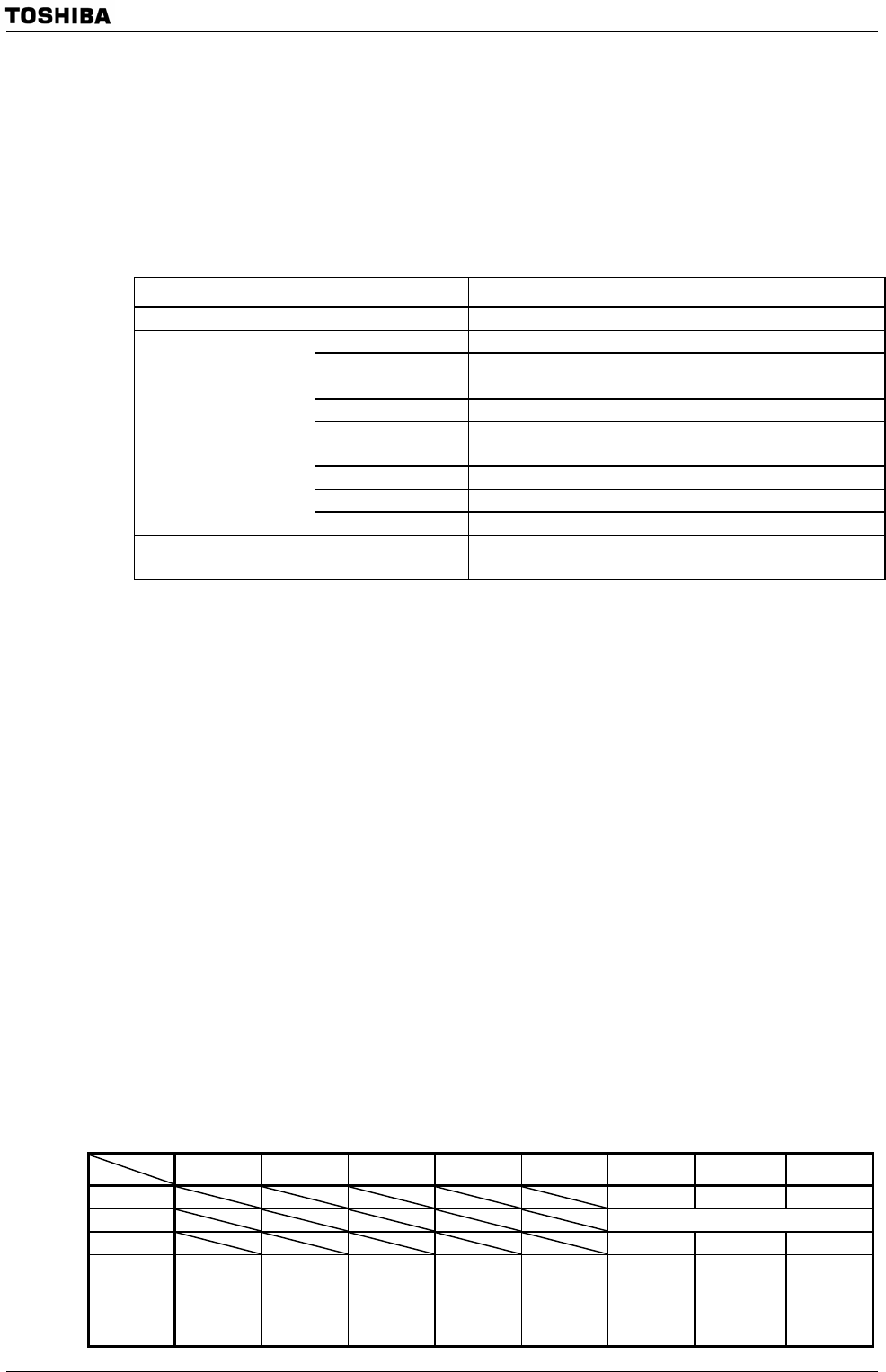
Table 3.25.1 Wake-up triggers
Source Symbol Note
RTC INTRTC
INT0 Only support "Rising Edge"
INT1 Only support "Rising Edge"
INT2 Only support "Rising Edge"
INT3 Only support "Rising Edge"
INT4
When TSI, need to disable de-bounce circuit
Only support "Rising Edge"
INT5 Only support "Rising Edge"
INT6 Only support "Rising Edge"
External
INT7 Only support "Rising Edge"
Key INTKEY
KI0~KI8
Only support "Falling Edge"
When an interrupt request is accepted, the power management signals (PWE) changes from
“0” to “1” and power is supplied to each block that has been cut off. After the warm-up time set
in PMCCTL<WUTM1:0> has elapsed, HOT_RESET is automatically released and the CPU
starts up from the internal boot ROM regardless of the external AM pin state. All external
ports retain the state before entering the Power Cut Mode except for the PnDR setting which
is released upon release of HOT_RESET.
* Output pin Hi-Z state → “1” or “0” output
* Input pin input gate OFF → Input pin input gate ON
The internal boot ROM first checks the PMCCTL <PCM_ON> bit in the PMC. If this bit is
set to “1”, execution jumps to address 46000H in the internal RAM before making all initial
settings. The <PCM_ON> bit in the PMC is cleared to “0” by software.
Note 1: The interrupt that released the Power Cut Mode, whichever it is, does not activate any interrupt operation. Nor
is it possible to identify which interrupt released the Power Cut Mode.
Note 2: Once the PMCCTL<PCM_ON> bit is set to “1”, it remains in this state. To re-enter the Power Cut Mode, it is
necessary to set this bit to “0” once and then to “1” again. At this time, a minimum of 31 us must be inserted
between setting <PCM_ON> to “0” and “1”.
Note 3: Since the Power Cut Mode is exited using the boot ROM, some settings must be made by software. Be
careful about this point.
7 6 5 4 3 2 1 0
Bit symbol CSDIS ROMLESS VACE BROMCR
(016CH)
Read/Write R/W
After reset 1 0 1
Function
NAND Flash
area CS
output
0: Enable
1: Disable
Boot ROM
0: Used
1: Not used
Vector
address
conversion
0: Disable
1: Enable