
Micro Controller User's Manual


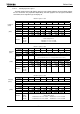


Table Of Contents
- TMP92CZ26AXBG
- 1. Outline and Features
- 2. Pin Assignment and Pin Functions
- 3. Operation
- 3.1 CPU
- 3.2 Memory Map
- 3.3 Clock Function and Standby Function
- 3.4 Boot ROM
- 3.5 Interrupts
- 3.6 DMAC (DMA Controller)
- 3.7 Function of ports
- 3.7.1 Port 1 (P10 to P17)
- 3.7.2 Port 4 (P40 to P47)
- 3.7.3 Port 5 (P50 to P57)
- 3.7.4 Port 6 (P60 to P67)
- 3.7.5 Port 7 (P70 to P76)
- 3.7.6 Port 8 (P80 to P87)
- 3.7.7 Port 9 (P90 to P92, P96, P97)
- 3.7.8 Port A (PA0 to PA7)
- 3.7.9 Port C (PC0 to PC7)
- 3.7.10 Port F (PF0 to PF5, PF7)
- 3.7.11 Port G (PG0 to PG5)
- 3.7.12 Port J (PJ0 to PJ7)
- 3.7.13 Port K (PK0 to PK7)
- 3.7.14 Port L (PL0 to PL7)
- 3.7.15 Port M (PM1, PM2, PM7)
- 3.7.16 Port N (PN0 to PN7)
- 3.7.17 Port P (PP1 to PP7)
- 3.7.18 Port R (R0 to R3)
- 3.7.19 Port T (PT0 to PT7)
- 3.7.20 Port U (PU0 to PU7)
- 3.7.21 Port V (PV0 to PV4, PV6, PV7)
- 3.7.22 Port W (PW0 to PW7)
- 3.7.23 Port X (PX4, PX5 and PX7)
- 3.7.24 Port Z (PZ0 to PZ7)
- 3.8 Memory Controller (MEMC)
- 3.9 External Memory Extension Function (MMU)
- 3.10 SDRAM Controller (SDRAMC)
- 3.11 NAND Flash Controller (NDFC)
- 3.11.1 Features
- 3.11.1 Block Diagram
- 3.11.2 Operation Description
- 3.11.3 ECC Control
- 3.11.4 Description of Registers
- 3.11.5 An Example of Accessing NAND Flash of SLC Type
- 3.11.6 An Example of Accessing NAND Flash of MLC Type (When the valid data is processed as 518byte)
- 3.11.7 An Example of Connections with NAND Flash
- 3.12 8 Bit Timer (TMRA)
- 3.13 16 bit timer / Event counter (TMRB)
- 3.14 Serial Channels (SIO)
- 3.15 Serial Bus Interface (SBI)
- 3.16 USB Controller
- 3.16.1 Outline
- 3.16.2 900/H1 CPU I/F
- 3.16.3 UDC CORE
- 3.16.3.1 SFRs
- 3.16.3.2 EPx_FIFO Register (x: 0 to 3)
- 3.16.3.3 bmRequestType Register
- 3.16.3.4 bRequest Register
- 3.16.3.5 wValue Register
- 3.16.3.6 wIndex Register
- 3.16.3.7 wLength Register
- 3.16.3.8 Setup Received Register
- 3.16.3.9 Current_Config Register
- 3.16.3.10 Standard Request Register
- 3.16.3.11 Request Register
- 3.16.3.12 DATASET Register
- 3.16.3.13 EPx_STATUS Register (x: 0 to 7)
- 3.16.3.14 EPx_SIZE Register (x: 0 to 7)
- 3.16.3.15 FRAME Register
- 3.16.3.16 ADDRESS Register
- 3.16.3.17 EOP Register
- 3.16.3.18 Port Status Register
- 3.16.3.19 Standard Request Mode Register
- 3.16.3.20 Request Mode Register
- 3.16.3.21 COMMAND Register
- 3.16.3.22 INT_Control Register
- 3.16.3.23 USB STATE Register
- 3.16.3.24 EPx_MODE Register (x: 1 to 3)
- 3.16.3.25 EPx_SINGLE Register
- 3.16.3.26 EPx_BCS Register
- 3.16.3.27 USBREADY Register
- 3.16.3.28 Set Descriptor STALL Register
- 3.16.3.29 Descriptor RAM Register
- 3.16.4 Descriptor RAM
- 3.16.5 Device Request
- 3.16.6 Transfer mode and Protocol Transaction
- 3.16.7 Bus Interface and Access to FIFO
- 3.16.8 USB Device answer
- 3.16.9 Power Management
- 3.16.10 Supplement
- 3.16.11 Points to Note and Restrictions
- 3.17 SPIC (SPI Controller)
- 3.18 I2S (Inter-IC Sound)
- 3.19 LCD Controller (LCDC)
- 3.20 Touch Screen Interface (TSI)
- 3.21 Real time clock (RTC)
- 3.22 Melody / Alarm generator (MLD)
- 3.23 Analog-Digital Converter (ADC)
- 3.23.1 Control register
- 3.23.2 Operation
- 3.23.2.1 Analog Reference Voltages
- 3.23.2.2 Analog Input Channel(s) selection
- 3.23.2.3 Starting an AD Conversion
- 3.23.2.4 AD Conversion Modes and AD Conversion-End Interrupts
- 3.23.2.5 High-Priority Conversion Mode
- 3.23.2.6 AD Monitor Function
- 3.23.2.7 AD Conversion Time
- 3.23.2.8 Storing and Reading the AD Conversion Result
- 3.23.2.9 Data Polling
- 3.24 Watchdog Timer (Runaway detection timer)
- 3.25 Power Management Circuit (PMC)
- 3.26 Multiply and Accumulate Calculation Unit (MAC)
- 3.27 Debug Mode
- 4. Electrical Characteristics
- 4.1 Maximum Ratings
- 4.2 DC Electrical Characteristics
- 4.3 AC Characteristics
- 4.3.1 Basic Bus Cycle
- 4.3.2 Page ROM Read Cycle
- 4.3.3 SDRAM controller AC Characteristics
- 4.3.4 NAND Flash Controller AC Characteristics
- 4.3.5 Serial channel timing
- 4.3.6 Timer input pulse (TA0IN, TA2IN, TB0IN0, TB1IN0)
- 4.3.7 Interrupt Operation
- 4.3.8 USB Timing (Full-speed)
- 4.3.9 LCD Controller
- 4.3.10 I2S Timing
- 4.3.11 SPI Controller
- 4.4 AD Conversion Characteristics
- 5. Table of Special function registers (SFRs)
- 6. Package

TMP92CZ26A
92CZ26A-210
3.9.2.2 LCD display bank register
The bank page used as LCD display memory is set to these registers. Since the bank register
for CPU and LCDC are prepared independently, the bank page for CPU (Program, Read-data,
write-data) can change during LCD display on.
LOCAL-X register for LCD
7 6 5 4 3 2 1 0
bit Symbol X7 X6 X5 X4 X3 X2 X1 X0
Read/Write R/W
After reset 0 0 0 0 0 0 0 0
Function Set BANK number for LOCAL-X (“0” is disabled because of overlapped with Common-area.)
15 14 13 12 11 10 9 8
bit Symbol LXE X8
Read/Write R/W R/W
After reset 0 0
Function
BANK for
LOCALX
0: Disable
1: Enable
Set BANK number for LOCAL-X
X8-X0 setting and CS
000000000∼011111111 CSXA
100000000∼111111111 CSXB
LOCAL-Y register for LCD
7 6 5 4 3 2 1 0
bit Symbol Y5 Y4 Y3 Y2 Y1 Y0
Read/Write R/W
After reset 0 0 0 0 0 0
Function
Set BANK number for LOCAL-Y
(“3” is disabled because of overlapped with Common-area.)
15 14 13 12 11 10 9 8
bit Symbol LYE
Read/Write R/W
After reset 0
Function
BANK for
LOCALY
0: Disable
1: Enable
LOCAL-Z register for LCD
7 6 5 4 3 2 1 0
bit Symbol Z7 Z6 Z5 Z4 Z3 Z2 Z1 Z0
Read/Write R/W
After reset 0 0 0 0 0 0 0 0
Function Set BANK number for LOCAL-Z (“3” is disabled because of overlapped with Common-area.)
15 14 13 12 11 10 9 8
bit Symbol LZE Z8
Read/Write R/W R/W
After reset 0 0
Function
BANK for
LOCALZ
0: Disable
1: Enable
Set BANK number for LOCAL-Z
Z8-Z0 setting and CS
000000000 to 001111111 CSZA 100000000 to 101111111 CSZC
010000000 to 011111111 CSZB 110000000 to 111111111 CSZD
LOCALLX
(888H)
(889H)
LOCALLY
(88AH)
(88BH)
LOCALLZ
(88CH)
(88DH)