
Datasheet


XTR106
2
SBOS092A
www.ti.com
I
O
= V
IN
• (40/R
G
) + 4mA, V
IN
in Volts, R
G
in Ω
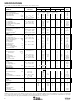
SPECIFICATIONS
At T
A
= +25°C, V+
= 24V, and TIP29C external transistor, unless otherwise noted.
XTR106P, U XTR106PA, UA
PARAMETER CONDITIONS MIN TYP MAX MIN TYP MAX UNITS
OUTPUT
Output Current Equation I
O
A
Output Current, Specified Range 4 20 ✻✻mA
Over-Scale Limit I
OVER
24 28 30 ✻✻✻ mA
Under-Scale Limit I
UNDER
I
REG
= 0, I
REF
= 0 1 1.6 2.2 ✻✻✻ mA
I
REF
+ I
REG
= 2.5mA 2.9 3.4 4 ✻✻✻ mA
ZERO OUTPUT
(1)
I
ZERO
V
IN
= 0V, R
G
= ∞ 4 ✻ mA
Initial Error ±5 ±25 ✻ ±50 µA
vs Temperature T
A
= –40°C to +85°C ±0.07 ±0.9 ✻✻ µA/°C
vs Supply Voltage, V+ V+ = 7.5V to 36V 0.04 0.2 ✻✻ µA/V
vs Common-Mode Voltage
(CMRR)
V
CM
= 1.1V to 3.5V
(5)
0.02 ✻ µA/V
vs V
REG
(I
O
) 0.8 ✻ µA/mA
Noise: 0.1Hz to 10Hz i
n
0.035 ✻ µAp-p
SPAN
Span Equation (Transconductance) S
S = 40/R
G
✻ A/V
Untrimmed Error Full Scale (V
IN
) = 50mV ±0.05 ±0.2 ✻ ±0.4 %
vs Temperature
(2)
T
A
= –40°C to +85°C ±3 ±25 ✻✻ ppm/°C
Nonlinearity: Ideal Input
(3)
Full Scale (V
IN
) = 50mV ±0.001 ±0.01 ✻✻ %
INPUT
(4)
Offset Voltage V
OS
V
CM
= 2.5V ±50 ±100 ✻ ±250 µV
vs Temperature T
A
= –40°C to +85°C ±0.25 ±1.5 ✻ ±3 µV/°C
vs Supply Voltage, V+ V+ = 7.5V to 36V ±0.1 ±3 ✻✻ µV/V
vs Common-Mode Voltage, RTI CMRR V
CM
= 1.1V to 3.5V
(5)
±10 ±50 ✻ ±100 µV/V
Common-Mode Range
(5)
V
CM
1.1 3.5 ✻✻V
Input Bias Current I
B
525 ✻ 50 nA
vs Temperature T
A
= –40°C to +85°C20 ✻ pA/°C
Input Offset Current I
OS
±0.2 ±3 ✻ ±10 nA
vs Temperature T
A
= –40°C to +85°C5 ✻ pA/°C
Impedance: Differential Z
IN
0.1 || 1 ✻ GΩ || pF
Common-Mode 5 || 10 ✻ GΩ || pF
Noise: 0.1Hz to 10Hz V
n
0.6 ✻ µVp-p
VOLTAGE REFERENCES
(5)
Lin Polarity Connected
to V
REG
, R
LIN
= 0
Initial: 2.5V Reference V
REF
2.5 2.5 ✻ V
5V Reference V
REF
55✻ V
Accuracy V
REF
= 2.5V or 5V ±0.05 ±0.25 ✻ ±0.5 %
vs Temperature T
A
= –40°C to +85°C ±20 ±35 ✻ ±75 ppm/°C
vs Supply Voltage, V+ V+ = 7.5V to 36V ±5 ±20 ✻✻ ppm/V
vs Load I
REF
= 0mA to 2.5mA 60 ✻ ppm/mA
Noise: 0.1Hz to 10Hz 10 ✻ µVp-p
V
REG
(5)
V
REG
5.1 ✻ V
Accuracy ±0.02 ±0.1 ✻✻ V
vs Temperature T
A
= –40°C to +85°C ±0.3 ✻ mV/°C
vs Supply Voltage, V+ V+ = 7.5V to 36V 1 ✻ mV/V
Output Current I
REG
See Typical Curves ✻ mA
Output Impedance I
REG
= 0mA to 2.5mA 80 ✻ Ω
LINEARIZATION
(6)
R
LIN
(external) Equation R
LIN
Ω
K
LIN
Linearization Factor K
LIN
V
REF
= 5V 6.645 ✻ kΩ
V
REF
= 2.5V 9.905 ✻ kΩ
Accuracy ±1 ±5 ✻✻ %
vs Temperature T
A
= –40°C to +85°C ±50 ±100 ✻✻ ppm/°C
Max Correctable Sensor Nonlinearity B V
REF
= 5V ±5 ✻ % of V
FS
V
REF
= 2.5V –2.5, +5 ✻ % of V
FS
POWER SUPPLY V+
Specified +24 ✻ V
Voltage Range +7.5 +36 ✻✻V
TEMPERATURE RANGE
Specification –40 +85 ✻✻°C
Operating –55 +125 ✻✻°C
Storage –55 +125 ✻✻°C
Thermal Resistance
θ
JA
14-Pin DIP 80 ✻ °C/W
SO-14 Surface Mount 100 ✻ °C/W
✻ Specification same as XTR106P, XTR106U.
NOTES: (1) Describes accuracy of the 4mA low-scale offset current. Does not include input amplifier effects. Can be trimmed to zero. (2) Does not include initial
error or TCR of gain-setting resistor, R
G
. (3) Increasing the full-scale input range improves nonlinearity. (4) Does not include Zero Output initial error. (5) Voltage
measured with respect to I
RET
pin. (6) See “Linearization” text for detailed explanation. V
FS
= full-scale V
IN
.
R
LIN
= K
LIN
• , K
LIN
in Ω, B is nonlinearity relative to V
FS
4B
1 – 2B