
Datasheet


XIO3130
www.ti.com
SLLS693F–MAY 2007–REVISED JANUARY 2010
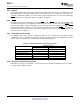
Figure 3-2. Power-Up Sequence Diagram
3.1.2 Power-Down Sequence
• Assert PERST to the device.
• Remove the reference clock.
• Remove 3.3-V and 1.5-V voltages.
See the power-down sequence diagram in Figure 3-3. If the VAUX33REF terminal is to remain powered
after a system shutdown, the switch power-down sequence is exactly the same as shown in Figure 3-3.
Figure 3-3. Power-Down Sequence Diagram
3.2 Express Interface
3.2.1 External Reference Clock
The Texas Instruments XIO3130 switch requires a differential 100 MHz common clock reference. The
clock reference must meet all PCI Express electrical specification requirements for frequency tolerance,
spread spectrum clocking, and signal electrical characteristics.
3.2.2 Clock Generator
The clock generator is responsible for generating all internal and external clocks from the PCI Express
reference clock. This includes the PHY transmitter serial link clock, the three downstream reference clock
outputs, the 60-kHz serial bus interface clock, and all internal clock domains.
Copyright © 2007–2010, Texas Instruments Incorporated Description 23
Submit Documentation Feedback
Product Folder Link(s): XIO3130