
Datasheet


XIO3130
www.ti.com
SLLS693F–MAY 2007–REVISED JANUARY 2010
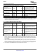
6.7 3.3-V I/O Electrical Characteristics
(1)
PARAMETER OPERATIONS TEST CONDITIONS MIN MAX UNIT
V
IH
High-level input voltage
(2)
V
DD33
0.7 V
DD33
V
DD33
V
V
IL
Low-level input voltage
(2)
V
DD33
0 0.3 V
DD33
V
V
I
Input voltage 0 V
DD33
V
V
O
Output voltage
(3)
0 V
DD33
V
t
p
Input transition time (trise and tfall) 0 25 ns
V
hys
Input hysteresis
(4)
0.13 V
DD33
V
V
OH
High-level output voltage V
DD33
I
OH
= –4 mA 0.8 V
DD33
V
V
OL
Low-level output voltage V
DD33
I
OL
= 4 mA 0.22 V
DD33
V
I
OZ
High-impedance, output current
(3)
V
DD33
V
I
= 0 to VDD33 ±20 mA
High-impedance, output current with internal
I
OZP
V
DD33
V
I
= 0 to VDD33 ±175 mA
pullup or pulldown resistor
(5)
I
I
Input current
(6)
V
DD33
V
I
= 0 to VDD33 ±1 mA
(1) This table applies to PERST, WAKE, REFCLK_SEL, GRST, and GPIO18:0.
(2) Applies to external inputs and bidirectional buffers.
(3) Applies to external outputs and bidirectional buffers.
(4) Applies to PERST and GRST.
(5) Applies to GRST (pullup resistor) and most GPIO (pullup resistor).
(6) Applies to external input buffers.
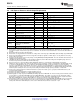
6.8 POWER CONSUMPTION
(1)
PARAMETER MIN NOM
(2)
MAX
(3)
UNIT
I
3.3V
11.21 20.61 mA
I
1.5V
578.7 725.8 mA
P
3.3V
36.99 68.01 mW
P
1.5V
868.05 1088.7 mW
I
AUX
(4)
5.28 mA
(1) Measurements taken at 25°C with nominal power supply, 3.3 V and 1.5 V.
(2) Nominal conditions are defined as switch only power, no devices downstream, and downstream clocks not running.
(3) Maximum power conditions are defined as three downstream devices constantly running traffic and downstream clocks running.
(4) Measurement performed with three devices downstream, system in S5.
6.9 THERMAL CHARACTERISTICS
PARAMETER TEST CONDITIONS
(1)
TYP UNIT
Low K JEDEC test board, 1s (single-signal layer), no air flow 51.2
No air flow 30.5
q
JA
Junction-to-free-air thermal resistance °C/W
High K JEDEC test board, 2s2p
400 LFM 17.7
(double-signal layer, double buried power plane)
200 LFM 14.7
q
JC
Junction-to-case thermal resistance Cu cold plate measurement process 7 °C/W
q
JB
Junction-to-board thermal resistance EIA/JESD 51-8 13.9 °C/W
Ψ
JT
Junction-to-top of package EIA/JESD 51-2 0.5 °C/W
Ψ
JB
Junction-to-board EIA/JESD 51-6 12 °C/W
(1) For more details, refer to TI application report IC Package Thermal Metrics (literature number SPRA953).
Copyright © 2007–2010, Texas Instruments Incorporated Electrical Characteristics 139
Submit Documentation Feedback
Product Folder Link(s): XIO3130