
Datasheet


INPUT VOLTAGE DYNAMIC RANGE
V =R I´
IN(PP) RG(PP)G
(9)
OUTPUT CURRENT AND VOLTAGE
R =
GMIN
=615.4W
3.2V
PP
5.2mA
PP
(10)
OUTPUT VOLTAGE DYNAMIC RANGE
BANDWIDTH
VCA822
www.ti.com
..................................................................................................................................... SBOS343C – SEPTEMBER 2007 – REVISED DECEMBER 2008
As illustrated in Equation 8 , once the output dynamic
range and maximum gain are defined, the gain
The VCA822 has a input dynamic range limited to
resistor is set. This gain setting in turn affects the
+1.6V and – 2.1V. Increasing the input voltage
bandwidth, because in order to achieve the gain (and
dynamic range can be done by using an attenuator
with a set gain element), the feedback element of the
network on the input. If the VCA822 is trying to
output stage amplifier is set as well. Keeping in mind
regulate the amplitude at the output, such as in an
that the output amplifier of the VCA822 is a
AGC application, the input voltage dynamic range is
current-feedback amplifier, the larger the feedback
directly proportional to Equation 9 .
element, the lower the bandwidth as the feedback
resistor is the compensation element.
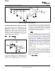
Limiting the discussion to the input voltage only and As such, for unity-gain or under-attenuated
ignoring the output voltage and gain, Figure 3 conditions, the input voltage must be limited to the
illustrates the tradeoff between the input voltage and CMIR of ± 1.6V (3.2V
PP
) and the current (I
RQ
) must
the current flowing through the gain resistor. flow through the gain resistor, ± 2.6mA (5.2mA
PP
).
This configuration sets a minimum value for R
E
such
that the gain resistor has to be greater than
Equation 10 .
The VCA822 provides output voltage and current
capabilities that are unsurpassed in a low-cost
monolithic VCA. Under no-load conditions at +25 ° C,
the output voltage typically swings closer than 1V to
either supply rails; the +25 ° C swing limit is within Values lower than 615.4 Ω are gain elements that
1.2V of either rails. Into a 15 Ω load (the minimum result in reduced input range, as the dynamic input
tested load), it is tested to deliver more than ± 160mA. range is limited by the current flowing through the
gain resistor R
G
(I
RG
). If the I
RG
current is limiting the
The specifications described above, though familiar in
performance of the circuit, the input stage of the
the industry, consider voltage and current limits
VCA822 goes into overdrive, resulting in limited
separately. In many applications, it is the voltage ×
output voltage range. Such I
RG
-limited overdrive
current, or V-I product, that is more relevant to circuit
conditions are shown in Figure 53 for the gain of
operation. Refer to the Output Voltage and Current
+10V/V and Figure 73 for the +100V/V gain.
Limitations plot (Figure 51 ) in the Typical
Characteristics. The X- and Y-axes of this graph
show the zero-voltage output current limit and the
zero-current output voltage limit, respectively. The With its large output current capability and its wide
four quadrants give a more detailed view of the output voltage swing of ± 3.9V typical on 100 Ω load, it
VCA822 output drive capabilities, noting that the is easy to forget other types of limitations that the
graph is bounded by a Safe Operating Area of 1W VCA822 can encounter. For these limitations, careful
maximum internal power dissipation. Superimposing analysis must be done to avoid input stage limitation,
resistor load lines onto the plot shows that the either voltage or I
RG
current; also, consider the gain
VCA822 can drive ± 2.5V into 25 Ω or ± 3.5V into 50 Ω limitation, as the control pin V
G
varies, affecting other
without exceeding the output capabilities or the 1W aspects of the circuit.
dissipation limit. A 100 Ω load line (the standard test
circuit load) shows the full ± 3.9V output swing
capability, as shown in the Typical Characteristics .
The output stage of the VCA822 is a wideband
The minimum specified output voltage and current current-feedback amplifier. As such, the feedback
over-temperature are set by worst-case simulations at resistance is the compensation of the last stage.
the cold temperature extreme. Only at cold startup do Reducing the feedback element and maintaining the
the output current and voltage decrease to the gain constant limits the useful range of I
RG
, and
numbers shown in the Electrical Characteristic tables. therefore reducing the gain adjust range. For a given
As the output transistors deliver power, the respective gain, reducing the gain element limits the maximum
junction temperatures increase, increasing the achievable output voltage swing.
available output voltage swing, and increasing the
available output current. In steady-state operation,
the available output voltage and current is always
greater than that temperature shown in the
over-temperature specifications because the output
stage junction temperatures are higher than the
specified operating ambient.
Copyright © 2007 – 2008, Texas Instruments Incorporated Submit Documentation Feedback 25
Product Folder Link(s): VCA822