
Datasheet


COMP
CS
CS
V
A 0 V 0.8 V
V
D
= £ £
D
(5) Gain is defined by: .
UCC2813-0, UCC2813-1, UCC2813-2, UCC2813-3, UCC2813-4, UCC2813-5
UCC3813-0, UCC3813-1, UCC3813-2, UCC3813-3, UCC3813-4, UCC3813-5
www.ti.com
SLUS161D –APRIL 1999–REVISED JUNE 2013
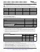
ELECTRICAL CHARACTERISTICS
Unless otherwise stated, these specifications apply for –40°C ≤ T
A
≤ +85°C for UCC2813-x; 0°C ≤ T
A
≤ +70°C for UCC3813-
x; VCC = 10 V
(1)
; RT = 100 k from REF to RC; CT = 330 pF from RC to GND; 0.1-µF capacitor from VCC to GND; 0.1-µF
capacitor from VREF to GND. T
A
= T
J
.
UCC2813-x
UCC3813-x
PARAMETER TEST CONDITIONS UNIT
MIN TYP MAX
Reference Section
Output voltage T
J
= 25°C, I = 0.2 mA, UCCx813-0 / -1 / -2 / -4 4.925 5 5.075
V
T
J
= 25°C, I = 0.2 mA, UCCx813-3 / -5 3.94 4 4.06
Load regulation 0.2 mA < I < 5 mA 10 30 mV
Total variation UCCx813-0 / -1 / -2 / -4
(2)
4.84 5 5.1
V
UCCx813-5, UCCx813-3
(2)
3.84 4 4.08
Output noise voltage 10 Hz ≤ f ≤ 10 kHz, T
J
= 25°C
(3)
70 µV
Long term stability T
A
= 125°C, 1000 Hours
(3)
5 mV
Output short circuit –5 –35 mA
Oscillator Section
Oscillator frequency UCCx813-0 / -1 / -2 / -4
(4)
40 46 52
kHZ
UCCx813-3 / -5
(4)
26 31 36
Temperature stability See
(3)
2.5 %
Amplitude peak-to-peak 2.25 2.4 2.55 V
Oscillator peak voltage 2.45 V
Error Amplifier Section
Input voltage COMP = 2.5 V; UCCx813-0 / -1 / -2 / -4 2.42 2.5 2.56
V
COMP = 2 V; UCCx813-3 / -5 1.92 2 2.05
Input bias current –2 2 µA
Open loop voltage gain 60 80 dB
COMP sink current FB = 2.7 V, COMP = 1.1 V 0.4 2.5 mA
COMP source current FB = 1.8 V, COMP = REF – 1.2 V –0.2 –0.5 –0.8 mA
Gain bandwidth product See
(3)
2 MHZ
PWM Section
Maximum duty cycle UCCx813-0 / -2 / -3 97 99 100
%
UCCx813-1 / -4 / -5 48 49 50
Minimum duty cycle COMP = 0 V 0 %
Current Sense Section
Gain See
(5)
1.1 1.65 1.8 V/V
Maximum input signal COMP = 5 V
(6)
0.9 1 1.1 V
Input bias current –200 200 nA
CS blank time 50 100 150 ns
overcurrent threshold 1.32 1.55 1.7 V
COMP to CS offset CS = 0 V 0.45 0.9 1.35 V
(1) Adjust VCC above the start threshold before setting at 10 V.
(2) Total Variation includes temperature stability and load regulation.
(3) Ensured by design. Not 100% tested in production.
(4) Oscillator frequency for the UCCx813-0, UCCx813-2, and UCCx813-3 is the output frequency.
Oscillator frequency for the UCCx813-1, UCCx813-4, and UCCx813-5 is twice the output frequency.
(6) Parameter measured at trip point of latch with Pin 2 at 0 V.
Copyright © 1999–2013, Texas Instruments Incorporated Submit Documentation Feedback 3
Product Folder Links: UCC2813-0 UCC2813-1 UCC2813-2 UCC2813-3 UCC2813-4 UCC2813-5 UCC3813-0
UCC3813-1 UCC3813-2 UCC3813-3 UCC3813-4 UCC3813-5